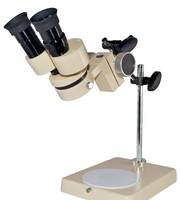
New RX-3 Stereo Microscope Features Eight-way Adjustable Pillar Stand
Includes binocular tube with diopter adjustment of +2 and variable, interpupillary adjustment. Provides inspection viewing for research, assembly, burring, electronic board soldering, miniature machine work and quality control inspections. Available in 20X eyepiece as well as 10X and 20X crosshair eyepiece options.
Read More »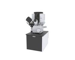
New Helios Hydra DualBeam System Allows Rapid Ion Beam Switching
Delivers four different ions as the primary beam, including argon, nitrogen, oxygen and xenon. Provides flexibility to analyze samples, improve results and develop improved materials. Suited for milling of carbon-based materials such as graphite used in battery anodes.
Read More »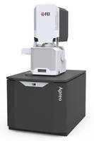
Scanning Electron Microscope supports diverse applications.
With compound final lens, Apreo™Ã- offers resolution down to 1.0 nm at 1 kV, without need for beam deceleration, for optimal performance on sampleÃ- even if it is tilted or topographic. Backscatter detection is offered at lowest beam currents, at any tilt angle, on sensitive samples, and at TV-rate imaging to maximize materials contrast, and detector segments can be individually...
Read More »
Mahr Federal to Feature MarVision MM 320 and MarVision QM 300 Video Measuring Microscopes with Image Processing at MD&M EAST 2016
Also on display will be the MarShaft™ SCOPE 250 plus flexible optical system for shop floor measurement PROVIDENCE, RI – Mahr Federal will feature the MarVision MM 320 and the MarVision QM 300 video measuring microscopes with image processing capability at MDM EAST, June 14-16, 2016, Jacob K. Javits Convention Center, New York, NY, Booth #2121. Designed for the measurement and/or dimensioning...
Read More »
Electric Aviation and a Sustainable Future
This white paper provides an in-depth overview into electric aviation and a sustainable future.
Read More »
FEI and CEOS Deliver First Sub-Angstrom, Low-Voltage Electron (SALVE) Microscope to the University of Ulm
Developed in the frame of University Ulm's SALVE project, the microscope provides high-contrast, atomic-scale imaging of radiation-sensitive samples, such as graphene and organic materials. Hillsboro, Ore. and Heidelberg, Germany — FEI (NASDAQ: FEIC) and CEOS announced today that they have delivered the first sub-Ãâ¦ngstrom, low-voltage electron (SALVE) microscope to the University of...
Read More »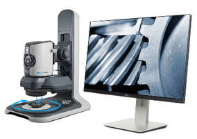
Digital Microscope offers full-HD 360-degree rotating views.
Designed for quality control, testing, inspection, and documentation, rotating viewer accessory for EVO Cam Digital Microscope delivers oblique view of subject that can be rotated 360Ã-
Read More »FEI and Oregon Health and Science University Install a Complete Correlative Microscopy Workflow in Newly Built Collaborative Science Facility
Installation is part of an expansion of the OHSU/FEI Living Lab for Cell Biology collaboration; a complete correlative microscopy solution will enable new approaches for cancer and related disease research Portland, Ore. –Ã- FEI (NASDAQ: FEIC) and Oregon Health and Science University (OHSU) today announced an expansion of their Living Lab for Cell Biology agreement that includes the...
Read More »Agilent Technologies Installs Atomic Force Microscope with Scanning Microwave Microscopy Capabilities at Cambridge Graphene Centre
SANTA CLARA, Calif.Ã- — Agilent Technologies Inc. (NYSE: A) today announced the recent installation of an Agilent 5600LS atomic force microscope at the Cambridge Graphene Centre (CGC) in the United Kingdom. The CGC, one of the key consortium partners in the ambitious Future and Emerging Technologies (FET) Graphene Flagship project, is directed by Andrea Ferrari, professor of nanotechnology...
Read More »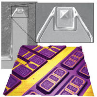
Atomic Force Microscopes sense both resistance and capacitance.
Based on shielded AFM probes and electronics from PrimeNano, Inc., sMIM Scanning Microwave Impedance Microscopy is integrated exclusively with MFP-3D™ and Cypher™ AFMs.Ã- Technique enables nanoscale mapping of permittivity and conductivity on linear and non-linear materials, including conductors, semiconductors, and insulators. sMIM is applicable to broad range of samples, including...
Read More »Probe Microphone can be used in small, hard-to-reach areas.
Accommodating R&D engineers who need to measure sound pressure in confined areas, Model 377B26 comprises microphone, preamplifier, housing, and probe tips of different lengths. Max operating temperature of 800Ã-
Read More »
Don't Let Your Money Drain Down the Hole...Drill Steel with Euroboor
As a globally recognized manufacturer of industrial grade portable tools, Euroboor is at the forefront of drilling and cutting technology. Our reputation as an industry leader is built on robust products that fit a wide range of industrial cutting and drilling applications. See our video to learn more about all of our quality products.
Read More »