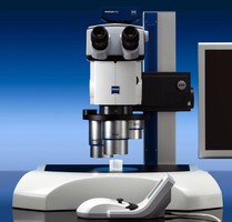
Stereomicroscope features high resolution visualization.
Model SteREO Discovery.V20 stereomicroscope enables users to visualize full specimens as well as smaller details within each specimen with one microscope. Features include 23 mm field of view at 10x, 20 to 1 available zoom range, step motor-controlled zoom optics, SyCoP system control panel, ergonomic design, Zeiss modular SetREO Discovery system integration, and compatibility with AxioCam...
Read More »
Microscopy System enables laser microdissection.
Suited for life science research, PALM MicroBeam IV extracts small biomaterials from heterogeneous tissue and cell colonies. Laser microdissection and pressure catapulting process provides pure and contact-free optical technique that is gentle enough to facilitate microdissection and manipulation of living cells in culture. Able to adjust to variety of source material, microscope offers inverted...
Read More »Laser Repair System allows for turnkey integration.
Optimized for high g-force gantry operation to 3g, QuikLaze 200 and BDS1000 industrial microscope combine to create optomechanical platform that features bolt-on installation. Along with beam-shaping true color optics, beam delivery system, and camera port, FPD system offers selectable repetition rates from single shot to 50 Hz continuous, Tri-lite beam blending configurations, and rotational X-Y...
Read More »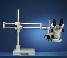
Luxo Expands 3-Day Quick-Ship Program to Include System 273 Microscopes
Elmsford, NY, June 2007 - Luxo has announced the expansion of its 3-Day Quick-Ship Program to include new top-selling System 273 Microscopes. The 23mm Microscopes included in the 3-Day Quick-Ship Program are Models 23714, 23714RB, 23712 and 23712RB. These System 273 Microscopes offer 25% greater magnification, 15% greater field of view and 20% greater working distance than traditional models....
Read More »
Rack System Design & Buyer's Guide
There is plenty to consider before setting up or replacing storage rack systems in your warehouse. This whitepaper contains a guide and general checklist of the most important considerations.
Read More »Stereo Microscope is designed for production/assembly.
GL Series Stereo Microscope features parfocal zoom magnification to minimize fatigue as well as side-mounted zoom controls and low positioned focus controls, allowing users to work in natural position. System offers working distance of at least 100 mm and zoom magnification ratios up to 9:1. Reticles or auxiliary lenses are available, as are multiple stand and lighting options.
Read More »Microscope bridges optical and scanning electron microscopy.
Facilitating operation via interactive touchscreen, Phenom(TM) can be used in most locations and does not require specialized facilities. Solution yields magnification up to 20,000x in compact design to bring high-resolution imaging to industrial as well as academic applications. Example areas of use include quality assurance, product development, research, and teaching.
Read More »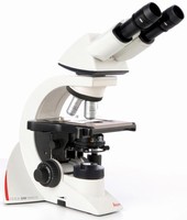
Microscope uses 4 W LED for color-neutral illumination.
Suited for clinical and biomedical laboratory use, Leica DM1000 LED features ergonomic design with options that can adapt to physical build and operating habits of individual users. Objectives are brightness-synchronized to protect eyes, diaphragm adjustment is color-coded, and rounded hard ceramic stage can be equipped with specimen holders. Optional portable solar power supply is available for...
Read More »High Resolution Microscope magnifies up to 20,000x.
Phenom(TM) high-resolution imaging microscope features performance levels between those of optical and scanning electron microscopes. Capable of yielding magnification up to 20,000x, unit features interactive touch screen user interface. Suitable applications include quality assurance, product development, research, and teaching. Unit is portable and requires no specialized facilities.
Read More »STEM System analyzes multiple wafer samples.
Designed for semiconductor labs, Expida(TM) 1255S DualBeam(TM) System integrates STEM Scanning/Transmission Electron Microscopy sample preparation with high-resolution imaging and analysis in single tool. It features ion beam column for preparing TEM samples, and electron column with 14-segment STEM detector for 30 kV imaging. System assures correct end-pointing and precise lamella thickness by...
Read More »Microscope Inspection System includes USB 2.0 camera.
Based on zoom optics, Model NAT-31 42X-540X resolves features 1 micron or less when added to probe station. Zoom optics have 0.7-4.5X objective lens, providing magnification of 42-270X for probe placement and device under test alignment with standard 0.5X auxiliary lens. Removal of auxiliary lens changes range of magnification to 84-540X for inspection and fine geometry probing. Working distance...
Read More »
Acoustic and Thermal Solutions for Original Equipment Manufacturers
Technicon's products solve the most complex noise pollution and thermal problems and improve product marketability. Check out the video to learn more.
Read More »