Strip System can be configured with 2 dual-wafer modules.
Suited for high-volume manufacturing at 90 nm node and below, Suprema 300 mm Strip System is based on modular design that makes it suited for development and production environments. Vacuum and atmospheric robots deliver throughput greater than 300 wafers/hr, and vacuum robot is capable of transferring 4 wafers simultaneously. Inductively coupled plasma source provides strip rates over 9...
Read More »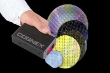
Reader tracks semiconductor wafers through manufacturing.
Featuring image formation technology and OCR, 2D matrix, and barcode recognition algorithms, In-SightÃ-® 1721 delivers reliable reading performance on SEMI-standard scribes. It can read wafer marks that have been affected by CMP, edge beads, copper metallization, and blue or green nitride coating. GUI facilitates set up, and automatic tuning minimizes operator intervention. Built-in network...
Read More »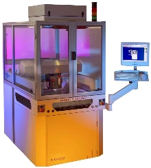
Dispensing System can be configured to suit application.
XyflexPro+ features advanced composite gantry design structure and linear drive system utilizing motion control drive technology. Platform, available as standalone or in-line system, offers flexibility to be configured for various dispense applications within electronics, automotive, and medical industries.
Read More »Power Delivery System suits semiconductor etch applications.
Fully integrated VHF Ovation(TM) delivers power up to 2.7 kW at fixed 60 MHz. It features onboard plasma measurement and enables fast, high-precision processes such as those required for sub-90 and sub-65 nm etch applications. Compact, half-rack unit delivers power into non 50 ohm environment without external sensor. It includes embedded voltage and current measurement technology for real-time...
Read More »
A Guide to Custom Water Manifold Assemblies
This white paper provides a guide to custom water manifold assemblies.
Read More »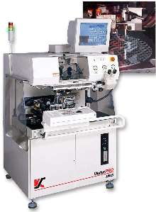
Stud Bumper handles 12 in. wafers in one pass.
WaferPRO plus single-pass stud bumper bonds 22 bumps/sec, depending on bump type, size, and pitch. It offers +5 Ã-µm positional accuracy at 3 sigma and can bump down to 65 Ã-µm. Various manual chucks and fully automatic wafer handling options are available. WaferPRO plus kit, which includes hardware, specialized servo code, and motion profiles, provides upgrade path for existing WaferPRO...
Read More »
Wet Process Station suits semiconductor applications.
Series 1412 Wet Process Station features safety-oriented design for clean appearance and chemical resistance. It comes in stainless steel, white polypropylene, and fire-retardant white polypropylene. Standard sizes range up to 8 ft wide x 42 in. deep, with other sizes available upon request.
Read More »Single-Reticle Pod transports and stores 150 mm reticles.
RSP-150 SMIF-POD(TM) features metal-free, gasket-sealed construction minimizing opacity, particle contamination, and drying time, while maximizing cleanability without disassembly. Streamlined design increases storage density. Optional AdvanTag(TM) tracking system with integrated RFID ties into socket built into unit to enable snap-on use of RFID transponder pill. For use in 300 mm fabs, optional...
Read More »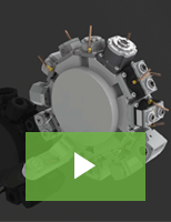
Von Ruden's Driven Tools Are Built to Last
Von Ruden's driven tools are designed to each specific machine in order to maximize performance. All of our tools are performance tested and made in the USA per ISO 9001:2015 standards. Check out our video to learn more.
Read More »