Micro IC Package targets mobile applications.
Building on micro SMD, micro SMDxt integrated circuit package enables design of products with bump counts of 42-100 bumps at 0.5 mm pitch without any underfill. Package height of 0.65 mm enables integration into thin-profile consumer products. Epoxy back coating protects against silicon damage during manufacturing, while self-aligning solder bumps facilitate surface mount assembly and rework.
Read More »Lead-Free IC Package offers green-certified solution.
Optimized for lead-free manufacturing, package integrates HysolÃ-® GR828H mold compound with Hysol QM1519 die attach adhesive for wire sweep properties and adhesive strength, respectively. Green solution, designed for 16- and 14-lead, Pb-free SOIC packages, uses Cu/Ni/Au leadframe. It achieves MRT reliability for MSL L1 up to 260Ã-
Read More »Ceramic Packages suit direct PCB mount applications.
Plated Copper on Thick Film technology permits manufacture of leadless ceramic chip carriers and packages larger than .75 in. Wrap-around interconnections eliminate use of leads and additional interface boards, and ensure connections can operate at frequencies above 32 GHz. Plugged via holes with resistance less than 1 mΩ provide for RF losses below .1 dB at 4 GHz. Depending on die size and...
Read More »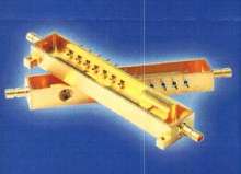
RF/Fiber Optic Packages handle harsh environments.
Unibody RF/Fiber Optic Packages are available with fully machined tubes and packages or packages with brazed tubes. Connecting tubes are copper, stainless steel, or Kovar and package material is stainless or Kovar. All types achieve temperature rating of 850Ã-
Read More »
Pressure Vessels & Their Components
This white paper provides an in-depth look into custom fabricated pressure vessels and their components.
Read More »IC Packaging is suited for analog products.
NanoStar(TM) wafer chip-scale packaging (WCSP) has no molding compound, lead frame, wire bonds, or leads. Using surface-mount technology assembly procedures, packaging can be mounted to PCB without additional under fill. Available power management ICs include RF LDO regulator; DC/DC buck converter; dual operational amplifier; audio power amplifier; and digital-to-analog converter with serial...
Read More »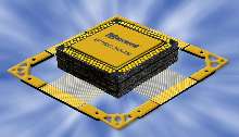
Packaging is hermetic and radiation shielded.
Rad-Stak(TM) vertically stacked packaging creates fully space-qualified components. Completely shielded, multi-level die package allows heat dissiplation through interconnects and lid/heat sink of each layer. Available in 132-pin and 68-pin outlines, packaging is applicable in multi-chip modules using identical die and true hybrids. Rad-Stak provides high-density, space-qualified SDRAM with...
Read More »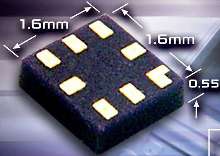
Multi-Terminal Logic Package measures 1.6 x 1.6 x 0.55 mm.
Utilizing encapsulated chip-on-substrate approach, MicroPak 8 consists of one 8-terminal chip scale leadless package for 1-, 2-, and 3-bit logic and switch functions. TinyLogicÃ-® MicroPak 8 package maintains 0.5 mm terminal pitch while its 0.2 x 0.3 mm land grid array contact pads ensure joint integrity under harsh environmental stresses. Currently offered is the UHS logic family which...
Read More »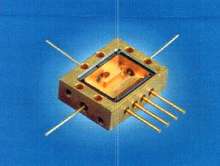
Modules deliver signal integrity up to 42 GHz.
Direct Bond-HF Modules utilize glass-to-metal sealing and Kovar housings. They maintain signal performance throughout all high frequency conductors without moding due to resistance. Modules are suitable for switches and multifunction chassis assemblies utilized in radar, early warning and countermeasure systems. Temperature performances exceed commercial and military standards and hermeticity is...
Read More »
Optimize Your Storage or Distribution Facility with Steel King Rack Solutions
Steel King racks are designed to meet seismic requirements in the most demanding conditions. Our durable storage products help your company save on maintenance costs. Check out our product video or download our Rack Planning eBook to learn more.
Read More »