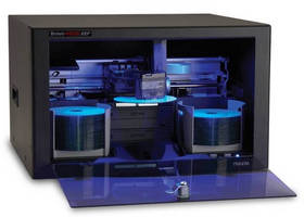
CD/DVD/BD Publishing Equipment delivers high-speed operation.
Available with 100 disc capacity and either 2 high-speed CD/DVD or CD/DVD/BD drives, Bravo 4102 XRP Disc Publisher prints full-color, 100% coverage disc in 6 sec. Built-in high-speed recorders, direct-to-disc printing, and robotics automate burning and printing of CDs, DVDs, and Blu-ray Disc(TM) media. Used for archival and distribution of video and audio, rack-mountable products feature...
Read More »Overland Storage Helps Leading University Graduate to Higher Levels of Data Protection with Innovative Tiered REO-NEO D2D2T Strategy
Washington and Lee University Embraces Overland's Disk- and Tape-Based Backup and Recovery Appliances to Lower Administrative Overhead, Extend Data Retention SAN DIEGO, Feb. 11 -- Overland Storage, Inc. (NASDAQ:OVRL) today announced that Washington and Lee University, a top-ranked college based in Lexington, Va., has deployed complementary REO SERIESÃ-® and NEO SERIESÃ-® disk- and...
Read More »Optical Disc Duplicators offer pushbutton operation.
Without requiring software, cables, or PC, Imation CD Duplicator and Imation CD/DVD Duplicator are compatible with 8 or 12 cm discs and feature LCD menu with functionality options. Both standalone disc-to-disc systems deliver continuous copying without need for cooling between duplications. While CD Duplicator operates on 52X CD-RW drive, CD/DVD Duplicator features 16X DVD+/-R/RW drive. Each...
Read More »D2D VTL Appliance promotes reliable backup and recovery.
Drop-in, disk-to-disk (D2D) virtual tape library (VTL) appliance, REO(TM) 4500, helps solve complex backup challenges while facilitating near-instantaneous data recovery. Along with 27 TB raw data capacity, solution supports SAS RAID controller, dual 4 Gbps FC and iSCSI host connectivity, as well as secure Web-based management. User-definable VTL offers RAID 5 protection and up to 6 library...
Read More »
The Legacy Automation Playbook
How to Proactively Manage Your Legacy Industrial Control System
Read More »Overland Storage Announces Availability of LTO4 Tape Drive Technology
SAN DIEGO, June 19 - Overland Storage, Inc. (NASDAQ:OVRL), a leading provider of tape- and disk-based backup and recovery solutions, has announced that its NEO Series and ARCvault families of tape automation will use HP fourth-generation linear open-tape drives, known as LTO4. HP was chosen as Overland's LTO4 tape drive supplier due to the relationship that exists between the two companies and...
Read More »GDA Collaborates with AMD to Develop Home Cinema Design
Innovative Home Entertainment Device Design Speeds Time to Market SAN JOSE, Calif., May 9, 2007 - GDA Technologies Inc., a leading Electronic Design Services (EDS) and Silicon Intellectual Property (SIP) solution provider for embedded, networking, and consumer electronics markets, today announced its successful collaboration with AMD to create a new reference design that OEMs can leverage to...
Read More »Backup System offers de-duplication and replication.
With scalable capacity up to 240 TB and performance up to 8 TB/hr, disk-based DXi7500 can serve as secure core repository for centralizing backup and disaster recovery from multiple distributed sites. Policy-based de-duplication offers in-line or post-process functionality based on requirements of each backup job. System offers option of integrated tape creation, allowing removable media to be...
Read More »Duplicator offers duplex printing.
With ability to print 2-sided documents with speed of 240 images/minute, Priport DX 4640PD digital printer features printing speed of 60-135 sheets/minute for 8.5 x 11 in. sizes and 60-120 sheets/minute for 11 x 17 in. sizes. Other features include 6 reduction and 5 enlargement ratios, 50-200% zoom, and scanning and printing resolutions of 600 x 400 and 400 x 400 dpi. Duplicator is equipped with...
Read More »CD and DVD Duplicator is equipped to handle large jobs.
Supplied with finely tuned firmware and software tested for compatibility and clean operation, OmniTower 11Ã-® features eleven NEC drives to accelerate completion of larger tasks. High-speed 16x DVD-R, 6x DVD+R Dual Layer, and 48x CD-R eliminate need for separate CD tower. Product also comes with Quick Start Guide and Operating Manual.
Read More »New Technologies: ICS Introduces a New Forensic Mac Acquisition Tool, a New CF Adapter for the IM4000 Product Family and Enhanced Hashing Support for the ImageMASSter Solo-3 Forensic Product
CHATSWORTH, Calif., May 21 / - Intelligent Computer Solutions (ICS) has announced today the release of new features to its hand-held Forensic Data Acquisition unit, the ImageMASSter Solo-3 Forensic. ICS also introduced a new Forensic Mac acquisition tool as well as the release of a new line of CF adapters to enhance the capabilities of the ICS line of Hard Drive duplicators. ICS has implemented...
Read More »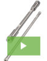
5 and 13 Micron Resolve Columns with Greater Bed Stability
Jordi Labs provides materials solutions that set the standard for innovation and quality. Our line of GPC and GFC columns are on the cutting edge of precision manufacturing and a result of our uncompromising commitment to quality and customer service. See our video to learn more.
Read More »