Wafer Inspection System finds defects in 22 nm devices.
Press Release Summary:
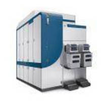
Applied UVision® 4 enables chipmakers to find defects in critical patterning layers of 22 nm and below logic/memory devices. Product combines DUV laser illumination, programmable polarization, and ultra-sensitive scattered light detectors to achieve optimal inspection sensitivity. Flexible optical system supports wide dynamic range detectors that allow all of chip to be imaged at once. Image processing engine enables data analysis at up to 12 billion pixels/sec.
Original Press Release:
Applied Materials Enables Defect Inspection at 22 nm and Below With New UVision 4 System
SANTA CLARA, Calif. - Applied Materials, Inc. today unveiled its Applied UVision® 4 wafer inspection system, enabling chipmakers to detect yield-limiting defects in the critical patterning layers of 22nm and below logic and memory devices. Extending Applied's successful DUV* laser imaging technology, the UVision 4 delivers the sensitivity and productivity needed to rapidly locate and identify defects previously unseen by any other inspection system.
"When coupled with our industry standard Applied SEMVision(TM) G4 defect review system, the UVision 4 offers chipmakers the fastest time from data to information, allowing them to resolve performance-limiting defect issues to boost yield and reduce cycle time."
The UVision 4 system is already the tool of record at multiple leading flash manufacturers where it is used for 32nm production and in the development of 22nm and EUV lithography processes. The UVision 4 has also played a key role in the development of 22nm SADP* technology at Applied's Maydan Technology Center.
"The critical challenge of finding and characterizing defects in the minute features created by the latest immersion lithography and double patterning techniques can only be met only with the innovations provided in the UVision 4 system," said Ronen Benzion, vice president and general manager of Applied's Process Diagnostics and Control division. "When coupled with our industry standard Applied SEMVision(TM) G4 defect review system, the UVision 4 offers chipmakers the fastest time from data to information, allowing them to resolve performance-limiting defect issues to boost yield and reduce cycle time."
Launched in 2005, the UVision platform propelled brightfield inspection into the DUV era by introducing simultaneous brightfield and scattered light (grayfield) DUV laser inspection to the semiconductor industry. Applied has now significantly advanced this breakthrough technology with the UVision 4 system, combining DUV laser illumination, programmable polarization and ultra-sensitive scattered light detectors to achieve benchmark inspection sensitivity.
The UVision 4 system's powerful, flexible optical system enables smaller pixel sizes, collects up to 40% more scattered light, and supports new wide dynamic range (WDR) detectors that allow all areas of a chip to be optimally imaged in a single scan. The new system also features key productivity enhancements, including a new image processing engine that improves data analysis speed to an impressive 12 billion pixels per second, delivering up to 35% higher wafer throughput than its predecessor.
Existing UVision users can take advantage of the new capabilities introduced in the UVision 4 via a convenient upgrade package, allowing chipmakers a rapid, cost-effective route to keep their defect inspection capabilities at the leading edge while using their existing fab assets. For more information on the UVision 4 system, visit appliedmaterials.com/products/uvision_4.html.
Applied Materials, Inc. (Nasdaq:AMAT) is the global leader in Nanomanufacturing Technology(TM) solutions with a broad portfolio of innovative equipment, service and software products for the fabrication of semiconductor chips, flat panel displays, solar photovoltaic cells, flexible electronics and energy efficient glass. At Applied Materials, we apply Nanomanufacturing Technology to improve the way people live. Learn more at www.appliedmaterials.com.
*DUV = deep ultra-violet; SADP = self-aligned double patterning