New VU19P Virtex UltraScale FPGA from Xilinx Enables Prototyping and Emulation
Press Release Summary:
- Comes with 35 billion transistors that provides logic density and I/O count on a single device
- Ideal for test, measurement, compute, networking, aerospace and defense-related applications
- Features 9 million system logic cells, up to 1.5 terabits per-second of DDR4 memory bandwidth and up to 4.5 terabits per-second of transceiver bandwidth, and over 2,000 user I/Os
Original Press Release:
Xilinx Announces the World's Largest FPGA Featuring 9 Million System Logic Cells
New Virtex UltraScale+ Device Enables the Creation of Tomorrow's Most Complex Technologies
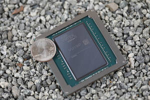
SAN JOSE, Calif., Aug. 21, 2019 /PRNewswire/ -- Xilinx, Inc. (NASDAQ: XLNX), the leader in adaptive and intelligent computing, today announced the expansion of its 16 nanometer (nm) Virtex® UltraScale+™ family to now include the world's largest FPGA — the Virtex UltraScale+ VU19P. With 35 billion transistors, the VU19P provides the highest logic density and I/O count on a single device ever built, enabling emulation and prototyping of tomorrow's most advanced ASIC and SoC technologies, as well as test, measurement, compute, networking, aerospace and defense-related applications.
The VU19P sets a new standard in FPGAs, featuring 9 million system logic cells, up to 1.5 terabits per-second of DDR4 memory bandwidth and up to 4.5 terabits per-second of transceiver bandwidth, and over 2,000 user I/Os. It enables the prototyping and emulation of today's most complex SoCs as well as the development of emerging, complex algorithms such as those used for artificial intelligence, machine learning, video processing and sensor fusion. The VU19P is 1.6X larger than its predecessor and what was previously the industry's largest FPGA — the 20 nm Virtex UltraScale 440 FPGA.
"The VU19P enables developers to accelerate hardware validation and begin software integration before their ASIC or SoC is available," said Sumit Shah, senior director, product line marketing and management, Xilinx. "This is our third generation of world-record FPGAs. First was the Virtex-7 2000T, followed by the Virtex UltraScale VU440, and now the Virtex UltraScale+ VU19P. But this is more than silicon technology; we're providing robust and proven tool flows and IP to support it."
The VU19P is supported by an extensive set of debug, visibility tools, and IP, providing customers with a comprehensive development platform to quickly design and validate next-generation applications and technologies. Hardware and software co-validation allows for developers to bring up software and implement custom features before physical parts are available. Moreover, the design flow can be co-optimized by using the Xilinx Vivado® Design Suite, which reduces cost and tape-out risk, and improves efficiency and time-to-market.
"Arm relies on Xilinx devices as part of our process for validating our next-generation processor IP and SoC technology," said Tran Nguyen, director of design services, Arm. "The new VU19P will further enable Arm, and many others in our ecosystem, to accelerate the design, development and validation of our most ambitious roadmap technologies."
The VU19P will be generally available in the fall of 2020. To learn more about the VU19P as well as Xilinx's complete line of Virtex UltraScale+ FPGA products, visit www.xilinx.com/products/silicon-devices/fpga/virtex-ultrascale-plus-vu19p.html.
About Xilinx
Xilinx develops highly flexible and adaptive processing platforms that enable rapid innovation across a variety of technologies – from the endpoint to the edge to the cloud. Xilinx is the inventor of the FPGA, hardware programmable SoCs, and the ACAP, designed to deliver the most dynamic processor technology in the industry and enable the adaptable, intelligent, and connected world of the future. For more information, visit www.xilinx.com.
PR Contact:
Tara Sims
media@xilinx.com
Xilinx, Inc.
Web Site: http://www.xilinx.com