New Image Sensor and Wafer-level Camera Module Features Small Pixel Size of 2.2 Microns
Press Release Summary:
- OC0VA wafer-level camera module combines sensor with image signal processing and optics into a 2.69 x 3.04 x 3.04mm
- OG0VA image sensor has a small form factor that results in a 2.69x3.04mm footprint for the OC0VA camera module
- Provides 640x480 VGA resolution at 240 fps and 320x240 QVGA resolution at 480 fps
Original Press Release:
OmniVision Expands Industry's Smallest BSI Global Shutter Pixel Family with New VGA Image Sensor and Wafer-level Camera Module
New Imagers Combine Nyxel® Technology, 2.2 Micron Pixel Size and Superior Near-Infrared Performance for Sharp, Accurate Images in Machine Vision and 3D Sensing Applications
Santa Clara, Calif., Jan. 3, 2020 /PRNewswire/ -- OmniVision Technologies, Inc., a leading developer of advanced digital imaging solutions, today announced in advance of CES the expansion of its backside-illuminated (BSI), global shutter (GS) sensor family with new VGA imagers that feature the industry's smallest pixel size of 2.2 microns—the OG0VA image sensor and OC0VA CameraCubeChip™ wafer-level camera module. Additionally, the OC0VA is the first CameraCubeChip with Nyxel® technology. Existing VGA global shutter devices have low near-infrared (NIR) quantum efficiency (QE) and high modulation transfer function (MTF) degradation, which requires a stronger light source with high power consumption and low performance. These new imagers feature OmniVision's PureCel®Plus-S stacked pixel architecture and Nyxel NIR technology to enable optimal performance and precision along with industry-leading QE and excellent MTF.
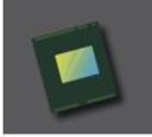
The OG0VA and OC0VA are ideal for a wide range of consumer and industrial machine vision and 3D sensing applications that need a global shutter to avoid motion blur, along with top NIR performance that reduces system power consumption by requiring less IR LED illumination in low- and no-light conditions. Target applications include facial authentication and eye tracking in smartphones and notebooks, as well as imaging for AR/VR headsets, drones and robots. These applications are also space constrained, and the OG0VA has a small form factor that results in a 2.69x3.04mm footprint for the OC0VA camera module, enabling thin and zero bezel phones, notebooks and tablets, along with smaller and lighter AR/VR glasses.
"There is a growing need for global shutter technology at a variety of resolution levels to accurately capture the images of moving objects, along with excellent NIR performance and small size," said Devang Patel, senior staff marketing manager for the security and emerging segments at OmniVision. "The OG0VA and OC0VA expand our family of the industry's smallest GS imagers by providing VGA resolution options with the best NIR performance in a global shutter device."
The OG0VA image sensor provides 640x480 VGA resolution at 240 frames per second (fps) and 320x240 QVGA resolution at 480 fps, in the industry's smallest optical format of 1/10 inches. The OC0VA CameraCubeChip combines this sensor with image signal processing and optics into a 2.69 x 3.04 x 3.04mm wafer-level camera module. Additionally, their low light sensitivity is excellent, with significantly lower gain than the industry's typical 3.0 micron pixel size for an improved signal-to-noise ratio.
These imagers' high MTF enables sharper images with greater contrast and more detail, which helps to enhance machine vision decision-making processes. They also have a high QE of 40% at 940nm and 60% at 850nm. This industry-leading QE enables the devices to see farther and better in low- and no-light conditions, which allows designers to use less IR LED light and achieve lower system-level power consumption. For AR/VR headsets, this reduces heat generation, while industrial and robotics applications can use fewer IR LEDs for lower system cost, or use the same number to achieve a greater image detection range.
Samples are expected in mid to late January for both the OG0VA image sensor and the OC0VA camera module. Additionally, this 2.2 micron Nyxel BSI GS technology will be demonstrated at OmniVision's CES hotel suite, from January 7-10. Contact your OmniVision sales representative for more information or to schedule a CES meeting: www.ovt.com/contact-sales.
About OmniVision
OmniVision Technologies, Inc. is a leading developer of advanced digital imaging solutions. Its award-winning CMOS imaging technology enables superior image quality in many of today's consumer and commercial applications, including mobile phones; security and surveillance; automotive; tablets, notebooks, webcams and entertainment devices; medical; and AR, VR, drones and robotics imaging systems. Find out more at www.ovt.com.
OmniVision®, CameraCubeChip™, Nyxel®, PureCel®, and the OmniVision logo are trademarks or registered trademarks of OmniVision Technologies, Inc. All other trademarks are the property of their respective owners.
Source OmniVision Technologies, Inc.
Contact:
Media Contact:
Eric Lawson
Kiterocket
+1 480.276.9572
elawson@kiterocket.com
Company Contact:
Mengxi Liu
OmniVision Technologies, Inc.,
+1 408.653.3484
mengxi.liu@ovt.com
Web Site: http://www.ovt.com