New 392x and 295x Optical Inspection Systems Achieve Unparalleled Levels of Sensitivity
Press Release Summary:
- Use different wavelength ranges to cover inspection applications for all layers
- eDR7380 e-beam wafer defect review system provides fast defect sourcing in development, fast excursion detection and more accurate, actionable data during production
- Designed to accelerate time-to-market for leading-edge 3D NAND, DRAM and logic integrated circuits (ICs) throughout their product lifecycle
Original Press Release:
KLA Announces New Defect Inspection and Review Portfolio
Strengthening KLA's Position in Patterned Wafer Defect Inspection, Review and Classification
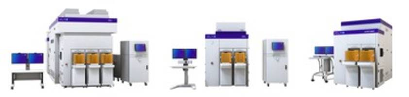
Milpitas, Calif., July 8, 2019 /PRNewswire/ -- Today KLA Corporation (NASDAQ: KLAC) announced the 392x and 295x optical defect inspection systems and the eDR7380™ e-beam defect review system. The new inspection systems are extensions of the company's flagship patterned wafer platforms, featuring advancements in the speed and sensitivity that define optical inspection. The new e-beam review system introduces innovations that cement its value as the essential link between defect and source. This portfolio is designed to accelerate time-to-market for leading-edge 3D NAND, DRAM and logic integrated circuits (ICs) throughout their product lifecycle.
"Manufacturing the next generation of memory and logic chips profitably requires unprecedented process control," said Ahmad Khan, executive vice president of the Global Products Group at KLA. "Device structures are smaller, narrower, taller and deeper, with more complex shapes and new materials. Discriminating defects from benign physical variations—signal from noise—has become an incredibly difficult problem. I'm excited to announce that our optical and e-beam engineering teams have developed a family of innovative, connected defect inspection and review systems, designed to enable our industry to continue to move forward."
The 392x and 295x optical patterned wafer defect inspection systems achieve unparalleled levels of sensitivity, throughput and yield-relevant binning by leveraging substantial advances in broadband plasma illumination technology, sensor architecture and integration of chip design information. As a result, the new systems provide faster defect discovery, accelerated yield learning, and more comprehensive inline monitoring than their industry-leading predecessors. The 392x and 295x systems use different wavelength ranges to cover inspection applications for all layers, from shallow trench isolation through metallization, including EUV lithography quality control.
With best-in-class image quality and the unique ability to deliver a complete defect pareto in one test, the eDR7380 e-beam wafer defect review system provides faster defect sourcing in development, faster excursion detection, and more accurate, actionable data during production. The system is equipped to support review of fragile EUV lithography process layers. Unique linkage to KLA inspectors reduces time to results, enables access to a broad range of KLA-specific applications, and improves inspection sensitivity through smart sampling and efficient exchange of defect data.
The 392x, 295x and eDR7380 systems are available as new systems or as upgrades from previous-generation 39xx, 29xx or eDR7xxx systems. These systems are designed for future extendibility to protect a fab's capital investment.
All of the new systems are in operation at leading IC manufacturers worldwide, where they work together to make innovative electronic devices manufacturable. To maintain the high performance and productivity demanded by chip manufacturers, the 392x, 295x and eDR7380 systems are backed by KLA's global comprehensive service network. More information about the new defect inspection and review systems can be found on the portfolio information page.
eDR® is a registered trademark of KLA Corporation.
About KLA:
KLA-Tencor Corporation (aka "KLA Corporation" or "KLA") develops industry-leading equipment and services that enable innovation throughout the electronics industry. We provide advanced process control and process-enabling solutions for manufacturing wafers and reticles, integrated circuits, packaging, printed circuit boards and flat panel displays. In close collaboration with leading customers across the globe, our expert teams of physicists, engineers, data scientists and problem-solvers design solutions that move the world forward. Additional information may be found at https://www.kla.com/ (KLAC-P).
Source KLA Corporation
Contact:
Investor Relations: Ed Lockwood, Sr. Director, Investor Relations (408) 875-9529, ed.lockwood@kla.com
Media Relations: Becky Howland, Ph.D., Sr. Director, Corporate Communications, (408) 875-9350, becky.howland@kla.com
Web Site: https://www.kla.com