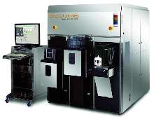
CD-SEM is suited for critical dimension metrology.
Share:
Press Release Summary:

With measurement throughput up to 1,000 sites/hr, Yosemite SP-1000 CD-SEM (Critical Dimension Scanning Electron Microscope) features clear imaging at bottom of 30:1 aspect ratio contact holes. System retains 3D model-based critical shape metrology required at and below 65 nm for accurate representation of physical shape of features. Unit uses landing energies as low as 100 eV. Product is suited for use in semiconductor manufacturing.
Original Press Release:
Soluris Introduces Yosemite SP-1000 CD-SEM for High Productivity Critical Dimension Metrology at 65nm and Beyond
Yosemite SP-1000 breaks records with system throughput as high as 1000 sites per hour and revolutionary performance on high aspect ratio contact holes.
Concord, MA - December 7, 2004 - Soluris, a manufacturer of CD-SEMs (Critical Dimension Scanning Electron Microscopes) for advanced semiconductor manufacturing, announced today the release of the new Yosemite SP-1000. Measurement throughput as high as 1000 sites per hour and clear imaging at the bottom of high aspect ratio contact holes are just two of the new system's performance features. The system retains the pioneering Ultra Low Voltage and 3-D model-based Critical Shape Metrology required at and below 65 nm. CD-SEMs are used by semiconductor manufacturers to measure and control the size of the smallest features created in their manufacturing processes.
"Productivity!" said Alain Bojarski, Soluris president and CEO when asked about the new system's most important benefit. "Productivity is the sum of process capability and throughput. Yosemite's unique performance at 65nm is proven. The Yosemite SP-1000 increases that capability to record-breaking throughputs - up to 1000 sites per hour. Our Beta customer reports throughput gains of as much as 3 times over our leading competitor in head-to-head comparisons on product wafers in a real fab environment. We have worked closely with this beta customer, a very large semiconductor manufacturer, for whom productivity, large sampling plans and high throughput are critical elements. Our customers are thrilled and excited by the system's ability to image and measure at the bottom of 30:1 aspect ratio contact holes."
"The 65nm node is a critical inflection point on the CD-SEM technology curve," added Neal Sullivan, Soluris vice president of technology. "The features we measure at this node are comparable in size to the distance that standard voltage electrons travel within the sample. In many ways, it is like the transformation that photolithography underwent when feature sizes became smaller than the wavelength of the illuminating light. Electron beam range in the sample must be shortened to adapt to tomorrow's geometries. Yosemite SP-1000 uses landing energies as low as 100eV, reducing electron range to less than one-tenth that of a conventional CD-SEM. Our 3-D model-based Critical Shape Metrology also provides a much more accurate representation of the physical shape of the feature than the intensity-based measurements of older technologies. Every nanometer of control on a 35nm gate translates directly into device performance and revenue dollars for our customers."
About Soluris
Soluris Inc., headquartered in Concord, MA, USA, has supplied instrumentation for optical and electron metrology since 1980, formerly as Schlumberger Verification Systems. With offices in North America, Europe and Asia, and a large international installed base, Soluris has the global reach and expertise to support installations worldwide. The group has been selected as a top-ten supplier of process diagnostic equipment in VLSI Research's 10 BEST Customer Satisfaction Survey in each of the last 5 years, including the #1 position in 2003 and 2004. With the introduction of its Yosemite CD-SEM, which won an R&D 100 award this year, Soluris has positioned itself as an innovative technology leader in next-generation model-based metrology. More information is available at www.soluris.com.
Contact: Paul C. Knutrud, Soluris Inc., +1 978-318-4041, pknutrud@soluris.com.


