Wafer Inspection System incorporates deep UV illumination.
Press Release Summary:
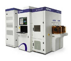
Leveraging DUV wavelength, special apertures, and multiple illumination and collection channels, Surfscan SP3 addresses stringent 28 nm node requirements for defect detection and classification on blanket films at production speeds. System helps manufacture substrates for 28 nm devices and below that are nearly atomically smooth and free from polish marks, crystalline pits, terracing, voids, or other defects that disrupt electrical integrity of transistor.
Original Press Release:
KLA-Tencor(TM) Announces New Surfscan® SP3 Defect and Surface Quality Inspection Systems for Substrate Manufacturing and IC Process Monitoring
Unique DUV-Driven Sensitivity, Industry-Leading Throughput Facilitate Manufacturing of Integrated Circuits at the 28nm Node and Below
MILPITAS, Calif., -- Today KLA-Tencor Corporation(TM) (NASDAQ: KLAC), announced a new generation in the Surfscan® family of wafer defect and surface quality inspection systems: the Surfscan SP3. As the first unpatterned wafer inspection platform to incorporate deep-ultraviolet (DUV) illumination, the Surfscan SP3 systems feature dramatic advances in sensitivity and throughput over their industry-benchmark predecessor, the Surfscan SP2XP. The Surfscan SP3 platform is also designed for extension to the next wafer size: 450mm.
"Launching a new Surfscan platform is an exciting event for KLA-Tencor," said Ali Salehpour, senior vice president and general manager of the Surfscan / ADE division at KLA-Tencor. "The visible-light Surfscan SP1 and the UV-illuminated Surfscan SP2 were well received by the industry; in fact, Surfscan tools can be found in every leading-edge substrate and chip manufacturing facility. Now we're announcing the first DUV unpatterned wafer inspection platform, to satisfy the industry's need for increased sensitivity at production speeds at the 28nm device node and below. We believe that the Surfscan SP3 will carry the Surfscan reputation for excellence in substrate and integrated circuit (IC) process tool qualification into the next generation."
The Surfscan SP3 system is designed to help develop and manufacture substrates for < 28nm devices that are nearly atomically smooth and free from polish marks, crystalline pits, terracing, voids or other defects that disrupt the electrical integrity of the transistor. Because these defects cannot be reliably detected by current-generation inspection systems at production speeds, substrate manufacturers have had difficulty achieving satisfactory yields with these top-grade, next-node wafers. KLA-Tencor's engineers have built the Surfscan SP3 inspection system with the DUV sensitivity and throughput needed to reliably identify critical defects and surface quality issues inline during substrate manufacturing.
In the IC fab, manufacturers must also be able to monitor rough and smooth unpatterned films after deposition and chemical mechanical polish (CMP) to ensure that process tools are not adding defects. The Surfscan SP3 leverages its unique DUV wavelength, special apertures and multiple illumination and collection channels to address stringent 28nm node requirements for defect detection and classification on blanket films at production speeds. The SP3 also offers a module that inspects the back side of wafers for defects that might deform the wafer shape during photolithography.
The extensive capabilities of the Surfscan SP3 are enabled by the following new features and improvements over the current-generation Surfscan platform:
-- Powerful DUV source and DUV-optimized optics, to help capture critical defects affecting devices at the 28nm node and below;
-- New stage and new image computer that, together with algorithm improvements, enable increased production throughput;
-- DUV-specific apertures that enhance defect capture on blanket films;
-- Integrated, high resolution (~100 mega-pixel), full-wafer SURFmonitor(TM) haze maps, providing automated capture of ultra-fine slip lines and scratches or maps of surface roughness, grain size and other process parameters; and
-- Defect coordinate accuracy improvements that enhance re-detection and speed of defect review and classification on KLA-Tencor's eDR electron-beam review tools, allowing engineers to track down the source of a defect excursion quickly and disposition wafers accurately.
Surfscan SP3 tools can be matched among themselves and correlated to the factory's existing Surfscan SP2 and SP2XP baselines, to enhance fleet flexibility and factory productivity. To maintain high performance and productivity, the Surfscan SP3 tools are backed by KLA-Tencor's global, comprehensive service network.
Surfscan SP3 systems have been shipped to leading substrate and chip manufacturers in Asia, the United States and Europe for use in advanced development and production lines. For more information on KLA-Tencor's unpatterned wafer defect inspection systems, please visit the product web pages at: www.kla-tencor.com/front-end-defect-inspection/surfscan-series.html.
About KLA-Tencor:
KLA-Tencor Corporation (NASDAQ: KLAC), a leading provider of process control and yield management solutions, partners with customers around the world to develop state-of-the-art inspection and metrology technologies. These technologies serve the semiconductor, data storage, LED, photovoltaic, and other related nanoelectronics industries. With a portfolio of industry-standard products and a team of world-class engineers and scientists, the company has created superior solutions for its customers for over 30 years. Headquartered in Milpitas, California, KLA-Tencor has dedicated customer operations and service centers around the world. Additional information may be found at www.kla-tencor.com. (KLAC-P)
CONTACT: Media Relations, Meggan Powers, Sr. Director, Corporate Communications, +1-408-875-8733, meggan.powers@kla-tencor.com
Web Site: www.kla-tencor.com