Logic Module prototypes up to 40 million ASIC gates capacity.
Share:
Press Release Summary:
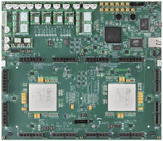
Based on 2 Xilinx 28 nm Virtex-7 FPGA devices, Dual 7V2000T TAI Logic Module provides up to 40 million ASIC gates of capacity and 1,200 external I/O on single board. Each board provides up to 32 GTX transceivers on specialized differential connectors and 6 programmable differential pair clocks running up to 700 MHz. Supporting all hardware control functions through USB and Gigabit Ethernet connections, module can run 2 GB of DDR2 and 4 GB of DDR3 memory at up to 800 and 1,333 MHz, respectively.
Original Press Release:
S2C Releases Dual Virtex-7 2000T FPGA Rapid SoC Prototyping Hardware
The New Dual 7V2000 TAI Logic Module Prototypes Up to 40 Million ASIC Gates Capacity
San Jose, Calif. - S2C Inc., a leading rapid SoC/ASIC prototyping solutions provider, announced its fifth-generation product, the Dual 7V2000T TAI Logic Module, first among the V7 family, based on two Xilinx's 28-nm Virtex-7 FPGA devices. The Dual V7 TAI Logic Module provides up to 40 million ASIC gates of capacity and 1,200 external I/O on a single board making it the world's most compact prototyping hardware for such a high gate capacity.
In addition to almost tripling the logic and memory capacity that can fit on a S2C's 4th generation Xilinx Virtex-6 and Altera Stratix-4 FPGA prototyping hardware, S2C's 5th generation products have many significant improvements to facilitate higher system prototype performance, reliability and ease-of-use through enhanced remote resource management, power management, clock management and cooling mechanisms. The new V7 TAI Logic Module now supports all the hardware control functions through both the USB and the new Gigabit Ethernet connections.
"We are pleased to be one of the first vendors to provide ASIC/SoC prototyping system based on the biggest FPGA, Xilinx Vitex-7 2000T, in the market today," noted Mon-Ren Chene, Chairman and CTO of S2C. "FPGA-based prototyping is becoming a critical step for a successful SoC product launch but was not a viable option for some design teams when their design sizes were extremely large and building a prototyping flow became too complex to manage. S2C's fifth generation product, based on the Virtex-7 based FPGA, is designed to make prototyping a pleasant experience for designs of any size from 20 Million up to 180 Million ASIC gates with 1 to 9 Xilinx Virtex-7 FPGAs on a single board. In addition, we provide a complete solution with prototype creation and debug software; DPI, SCE-MI and C-API co-modeling; and, a large library of Prototype Ready IP & Accessories."
The V7 TAI Logic Module series comes with a host of new capabilities both on hardware and software side, which significantly boosts the user productivity. On hardware side - each board provides a total of up to 32 GTX transceivers on specialized differential connectors; 6 programmable differential pair clocks capable of running up to 700 MHz; ability to remotely control the prototyping hardware through Gigabit Ethernet cable. On the software front new capabilities include - monitoring all on-board global clocks in real time, monitoring and displaying voltage, current and temperature; setting external I/O voltages through software, and provide global reset remotely through software. All V7 TAI Logic Modules are shipped with free TAI Player Pro runtime software that can be run on either Windows or Linux operating systems.
The V7 TAI Logic Modules can run both 2GB of DDR2 and 4GB of DDR3 memory at up to 800 and 1333 MHz respectively. S2C offers a large library of Prototype Ready(TM) IP and accessories including High Speed D/A and A/D, PCIe, Gigabit Ethernet, MIPI, SATA, ARM, SRAM, DDR2/3, Flash, TV Decoder/Encoder, Audio and DVI to further accelerate user's development of rapid FPGA based prototypes.
Availability
V7 TAI Logic Module is now shipping with XC7VLX2000T-ES FPGAs with lead time of approximately 8 to 12 weeks. The V7 TAI Logic Module can be mounted with either one or two FPGA devices per module. All V7 TAI Logic Modules adopt a similar form factor to all prior generation TAI Logic Modules, so that existing customers can easily upgrade and re-use their current daughter cards or mother boards.
S2C will be exhibiting the Dual V7 TAI Logic Module at DAC 2012 from Monday, June 3rd to Wednesday, June 6th at booth #414 at the 49th Design Automation Conference in San Francisco.
About S2C
Founded and headquartered in San Jose, California, S2C has been successfully delivering rapid SoC prototyping solutions since 2003. S2C provides:
o Rapid SoC FPGA-based prototyping hardware and automation software
o Prototype Ready(TM) IP, Platforms, and Accessories
o System-level design verification and acceleration
S2C's value is our singular focus on SoC/ASIC development. Our highly qualified engineering team and customer-focused sales force understands our customers' SoC development needs. S2C's unique FPGA-based solution, using our patented TAI IP technology, enables designers to quickly assemble FPGA-based SoC prototypes on S2C FPGA boards. This gives customers an early start on software development, typically the long pole item in development schedule. Combining rapid prototyping methodology with a comprehensive portfolio of Prototype Ready IP and advanced verification and acceleration solutions, S2C solutions greatly reduce the SoC design cycle.
In addition to the headquarters in San Jose, CA, S2C currently has 4 direct offices located in Shanghai, Beijing, Shenzhen China and Hsinchu, Taiwan. S2C is also the organizer of the annual SoCIP seminar and exhibition in China, which brings SoC designers from the Asia-Pacific region together with international silicon IP and SoC solution vendors. For more information, visit www.s2cinc.com.
Contacts for S2C:
Ashok Kulkarni, S2C Inc., San Jose. Phone: +1 408 213 8818 x820 Email: ashokk@s2cinc.com
Michel Cao, S2C Inc., Shanghai. Phone: +86 21 6887 9287, Email: michelc@s2cinc.com