Stable Measurement of Polished Targets Now Possible for ENR PWT

Photowatt, a pioneer in the solar-energy industry since 1979, uses Keyence's LK-G displacement sensor for high-precision detection of wafer thicknesses. In March 2012 the company was acquired by French utility EDF, via its EDF ENR subsidiary, now known as EDF ENR PWT.A wafer is a thin slice of semiconductor material, such as silicon, which generally measures between 200 and 300 microns in thickness. Wafers used in solar cells have a grid of electrical contacts that collect photovoltaic current (the metal portion visible on solar panels). When photons strike the cell, they knock away the electrons of the atoms contained in the cell material. Treating one side of the cell with a negatively charged substance and the other side with a positively charged substance allows these electrons to move and produce an electric current. The wafer is completed by placing a non-conductive layer between these two layers, which remain connected by a single wire.
"The wafers are arranged in a stack and then processed with a chemical treatment," says Grégory Glasson, Continual Improvement Coordinator at EDF ENR PWT. "One by one, the wafers are picked up by a robot, placed in an acid bath, and then washed. Because the wafers are very thin, the surface tension between adjacent wafers can result in two being picked up at the same time. Although this is infrequent—occurring at a rate of about 1 in every 5000 wafers—the issue is more than just product conformity. Our main concern is the safety of our staff because acid can remain between stuck wafers and come into contact with staff during handling."
"Detecting this issue is difficult because the 200-micron thickness of the wafers and uneven reflectance of its crystals make conventional inspection methods impossible. So I contacted Keyence. I knew about the performance of the LK-G displacement sensor because I had used one previously for a very complex application," adds Glasson.
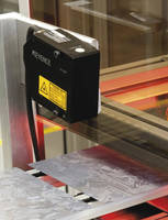
An LK-G head was installed on either side of the target to negate the impact of vibrations in the handling system which could distort the measurement. The dual head system resulted in highly accurate wafer thickness measurements for ENR PWT.
"As soon as we installed the LK-G, the values measured were extremely stable. We are now able to immediately detect whether wafers are stuck together," says Glasson.
The two sensor heads are connected to a single controller, so there was also a price savings compared to the many other dual head systems on the market.
Another challenge for performing this inspection is the speed of production. Since the silicon wafers are produced at one wafer per second, stable measurements need to be obtained quickly.
The LK-G offers accurate measurements (0.5 µm) at high sampling speeds, creating stable measurements. Although clear or translucent targets cause difficulty for conventional laser displacement sensors due to multiple reflections, the LK-G is equipped with two functions to overcome this problem. LK-G's ABLE function detects the target surface condition and automatically adjusts to maintain optimum laser intensity levels, achieving an adjustment range up to 90 times wider than conventional models. The MRC (Multiple Reflection Cancel) algorithm works in tandem to eliminate multiple reflections from shiny surfaces by comparing them against a standard waveform.
EDF ENR PWT designs and produces silicon photovoltaic modules start to finish, manufacturing every component from ingots, to wafers and cells. From day one, the company has set itself apart as an innovator with their ultra-high-efficiency solar cells designs. EDF ENR PWT is wholly owned by EDF ENR, France's leading name in rooftop photovoltaic systems for homes, businesses, and government entities. EDF ENR is a subsidiary of EDF Energies Nouvelles, a global green-electricity producer with a gross installed capacity of 4200 MW worldwide, primarily in wind and solar power.
www.keyence.com/edf
KEYENCE has steadily grown since 1974 to become an innovative leader in the development and manufacturing of automation equipment worldwide. Our products consist of automation sensors, static eliminators, barcode readers, measuring instruments, vision systems, laser markers, and digital microscopes.
Keyence Corporation of America
1100 North Arlington Heights Rd. Suite 210, Itasca, IL 60143
Phone: 1-888-KEYENCE (539-3623)
Fax: 1-201-930-0099
marketing@keyence.com


