Vision and Imaging Sensors / Detectors
ON Semiconductor Introduces RGB-IR Image Sensor and Hayabusa Family of CMOS Image Sensors
Press Release Summary:
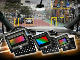
- 2.3 megapixel RGB-IR sensor achieves up to 120 dB dynamic range
- Hayabusa image sensor platform offers range of resolutions and imaging capabilities including options for embedded image signal processing
- 3.1 MP option with 8:3 wide aspect ratio makes it ideal for wide field-of-view applications
Original Press Release:
ON Semiconductor Showcases Automotive CMOS Image Sensors, LiDAR and Radar Solutions At AutoSens 2019
Complete automotive sensing portfolio on display, including sensors for in-cabin, rear view and surround view cameras, ADAS front view cameras, and camera monitor systems
Detroit, MI – May 14, 2019 – ON Semiconductor (Nasdaq: ON), driving energy efficient innovations, will demonstrate its comprehensive portfolio of sensors for automotive applications at the AutoSens Conference in Detroit, MI. At center stage will be the next-generation RGB-IR image sensor solution for in-cabin applications and the Hayabusa™ family of CMOS image sensors for advanced driver assistance systems (ADAS) and viewing automotive camera systems.
Designed to meet growing demand for in-cabin occupancy monitoring cameras, the 2.3 Megapixel (MP) RGB-IR sensor achieves up to 120 dB dynamic range and superior near infrared performance for high quality RGB images when visible light is present, and near infrared (NIR) enhanced images when the scene is actively illuminated with NIR light.
The Hayabusa image sensor platform has been expanded to offer a range of resolutions and imaging capabilities including options for embedded image signal processing. A 3.1 MP option with unique 8:3 wide aspect ratio makes it ideal for wide field-of-view applications such as front view ADAS to meet European New Car Assessment Program (NCAP) 2020 standards. With up to 60 frames per second capability, it also meets requirements for rear view electronic video mirrors, also known as class I camera monitor systems (CMS). The 1.3 MP option delivers a sensor and image signal processor in a single compact automotive qualified package, perfect for megapixel-based rear view cameras, surround view systems and automated parking systems where space constraints limit the camera body size.
“Automakers and suppliers are adding in-cabin safety and convenience features at an accelerated rate to meet new standards and provide expanded passenger experience. We are focusing on this emerging application with our diverse, high-performance in-cabin portfolio,” said Ross Jatou, Vice President and General Manager, Automotive Sensing Division, ON Semiconductor. “As the world’s first highly scalable family of automotive image sensors, ON Semiconductor’s Hayabusa family delivers exceptional performance in all lighting conditions and allows automakers to leverage the development of a core platform to create camera systems optimized for specific vehicle needs with faster time-to-market from engineering re-use.”
In addition to the Hayabusa family and RGB-IR sensor solution, ON Semiconductor will also demonstrate its LiDAR and radar technologies engineered for ADAS and autonomous driving. Visitors to AutoSens are also invited to attend a presentation by Wade Appelman, vice president of business development at SensL Division, Intelligent Sensing Group of ON Semiconductor, entitled “The Next Generation of SPAD Arrays for Automotive LiDAR”.
About ON Semiconductor
ON Semiconductor (Nasdaq: ON) is driving energy efficient innovations, empowering customers to reduce global energy use. The company is a leading supplier of semiconductor-based solutions, offering a comprehensive portfolio of energy efficient, power management, analog, sensors, logic, timing, connectivity, discrete, SoC and custom devices. The company’s products help engineers solve their unique design challenges in automotive, communications, computing, consumer, industrial, medical, aerospace and defense applications. ON Semiconductor operates a responsive, reliable, world-class supply chain and quality program, a robust compliance and ethics program, and a network of manufacturing facilities, sales offices and design centers in key markets throughout North America, Europe and the Asia Pacific regions. For more information, visit http://www.onsemi.com.
- Follow @onsemi on Twitter.
ON Semiconductor and the ON Semiconductor logo are registered trademarks of Semiconductor Components Industries, LLC. All other brand and product names appearing in this document are registered trademarks or trademarks of their respective holders. Although the company references its website in this news release, information on the website is not to be incorporated herein.
Contacts
Veronika Holscher
PR and Marketing Communications
ON Semiconductor
+1 (408) 660-2688
Parag Agarwal
Vice President Investor Relations and Corporate Development
ON Semiconductor
+1 (602) 244-3437