New Velocity Super EBSD Camera Provides Collection Speed up to 4,500 Indexed Points per Second
Press Release Summary:
- Integrated with compatible EDAX EDS detectors to provide analytical system for efficient simultaneous EDS-EBSD collection
- Image resolution, combined with proven EDAX triplet indexing routines, provides orientation precision values of less than 0.1°
- Enables high-speed mapping with the indexing performance on real-world materials
Original Press Release:
EDAX Launches New Velocityâ„¢ Super Electron Backscatter Diffraction (EBSD) Camera
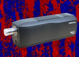
Mahwah, NJ, March 27, 2019 – AMETEK EDAX, Inc., a leader in X-ray microanalysis and electron diffraction instrumentation has added a new, faster, low-noise CMOS camera to its Velocity™ EBSD Camera Series. The Velocity™ Super is currently the fastest EBSD camera in the world, offering high-speed EBSD mapping with the highest indexing performance on real-world materials.
The Velocity™ EBSD Camera Series now includes two cameras tailored to specific EBSD analysis applications:
- Velocity™ Plus – collection speed up to 3,000 indexed points per second
- Velocity™ Super – collection speed up to 4,500 indexed points per second
Powered by a CMOS sensor, the Velocity™ EBSD Camera Series combines indexing speeds up to 4,500 indexed points per second with indexing success rates of 99% or better. At these speeds, the Velocity™ cameras use 120 x 120 pixel EBSD patterns for improved band detection. This image resolution, combined with proven EDAX triplet indexing routines, provides orientation precision values of less than 0.1°.
The Velocity™ EBSD cameras can be integrated with compatible EDAX EDS detectors to provide an analytical system for efficient simultaneous EDS-EBSD collection, even at the highest collection speeds. Furthermore, combining the collection with EDAX ChI-Scan™ analysis results in useful integrated data for accurate phase differentiation.
This new addition to the EDAX portfolio of EBSD cameras offers users another option for highspeed mapping and accurate indexing to resolve crystallographic microstructures and help solve materials characterization challenges quickly and easily.
For further information, please join our upcoming webinar, Applications of High-Speed CMOS Cameras for EBSD Microstructural Analysis, visit www.edax.com/velocity or email EDAX at info.edax@ametek.com.
About EDAX
EDAX is an acknowledged leader in Energy Dispersive Microanalysis, Electron Backscatter Diffraction and X-ray Fluorescence instrumentation. EDAX designs, manufactures, installs and services high-quality products and systems for leading companies in the semiconductor, metals, geological, pharmaceutical, biomaterials, and ceramics markets.
Since 1962, EDAX has used its knowledge and experience to develop ultra-sensitive silicon radiation sensors, digital electronics and specialized application software that facilitate solutions to research, development and industrial requirements.
EDAX is a unit of the Materials Analysis Division of AMETEK, Inc., which is a leading global manufacturer of electronic instruments and electromechanical devices with annual sales of approximately $5 billion.
For further information about EDAX, please contact:
Sue Arnell
EDAX, Inc.
91 McKee Drive, Mahwah, NJ 07430
Tel: (201) 529-4880
Fax: (201) 529-3156
E-mail: sue.arnell@ametek.com
Website: www.edax.com