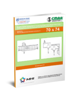
Mobility Tester measures electron mobility manually.
Share:
Press Release Summary:

Designed for semiconductor and solar manufacturing processes, LEI 1605 Mobility Tester measures electron mobility in range of ~300-20,000 cm2/v.sec through non-destructive contactless means on variety of substrates and materials. Sheet resistance is measured in range of 100 W-3 kW/square. Destructive Hall tests do not allow substrates to be recycled and reused. Featuring mapping capability, unit suits application in process development, prototyping, and small batch production.
Original Press Release:
Non-Destructive Hall Mobility Testing for Semiconductor, Solar Offered by Lehighton Electronics' New LEI 1605
February 23, 2009
Lehighton, Pennsylvania, USA -- Lehighton Electronics, Inc (LEI) announces the introduction of its new LEI 1605 Mobility Tester for semiconductor and solar manufacturing processes. The LEI 1605 manually measures electron mobility (EM) through a non-destructive contactless means on a variety of substrates and materials. The LEI 1605 is ideal for process development, prototyping, low-volume and small batch production. It is the newest product in Lehighton's line of mobility equipment geared toward universities and R&D centers. Its manual operation and thus lower cost make it an attractive and practical research alternative to the automatic, more expensive solutions that LEI offers for production volumes.
The LEI 1605 replaces the destructive van der Pauw Hall and Parallelepiped or Bridge Type methods currently used to achieve electron mobility, carrier density, carrier concentration and sheet resistance measures. The LEI 1605 provides critical, accurate process control measurements in situ. With the LEI 1605, researchers can measure electron mobility after each epitaxial layer deposition, enhancing their ability to monitor specific stages of process control. The LEI 1605 with optional upgrades will measure electron mobility in the range of ~300-20,000 cm2/v.sec, and will measure sheet resistance from ~100 W-3kW/square and possesses mapping capability.
The LEI 1605 reduces the cost of research by providing EM results instantly, allowing operators to make changes for optimal processing. The destructive Hall tests do not allow substrates to be recycled and reused; the LEI1605 eliminates this waste by allowing the reuse of wafers repeatedly. With this tool, there is no more cleaving, soldering and hoping for good connections and test results. This ultimately leads to more research of more concepts due to quick results, low risk factors, and low cost consumption. More research in shorter time with in-situ testing can lead to more projects and more funding.
About Lehighton Electronics Inc.
Lehighton Electronics Inc. has been engineering and providing metrology solutions to the silicon, compound semiconductor, solar, flat panel display and other related industries for more than 40 years. Some tools sold in the 1970s are still used in production today, providing our customers with consistently low tool ownership and operating costs.
For more information, visit lehighton.com; or contact
Robert Warren
at Lehighton Electronics Inc.,
P.O. Box 328,
Lehighton, PA 18235-0328 USA,
Tel. (800) 535-1112;
Outside the U.S., +717.917.6940;
Fax: (610) 377-6820;
Email at salesinfo@lehighton.com.