Axcelis Announces Multiple Wins for 'Purion XE' High Energy System Including New Foundry Penetration
Innovative Platform Delivers Industry Leading Purity, Precision and Productivity to Meet Future Process Challenges as Well as Today's Production Requirements BEVERLY, Mass.Ã- — Axcelis Technologies, Inc. (Nasdaq: ACLS), a leading supplier of enabling ion implantation solutions for the semiconductor industry, announced multiple wins for the Company's Purion XE single wafer, high energy...
Read More »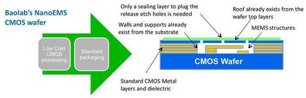
Process Allows Nanoscale MEMS to be created inside CMOS wafer.
NanoEMS(TM) technology enables construction of nanoscale MEMS (Micro Electro Mechanical Systems) within structure of actual CMOS wafer itself using standard, high-volume CMOS lines. Existing metal layers in CMOS wafer are used to form MEMS structure via standard mask techniques, and Inter Metal Dielectric is etched away using vapour HF. Etching uses equipment already available for volume...
Read More »
PBC Linear Uni-Guide Shines in Wafer Manufacturing
Rockford, IL - January 2, 2009 For Over 25 years, PBC Linear developed working relationships with its customers to help them save money and time by customizing PBC Linear products to their needs. From simple Pillow Block modification to a complex linear slides and stages, PBC Linear delivered on its expertise and the customer benefited with cost savings and rapid time to market! Class 10 clean...
Read More »
Rack Systems Done Right: A Hands-On Guide to Reaping Maximum Benefit from Design Review
Learn how to reap the maximum benefit from design review in our whitepaper.
Read More »BP Solar Introduces Mono2
New Silicon Growth Process Yields Higher Efficiency in Commercial Cells and Modules A pioneer in silicon casting for solar photovoltaic cell applications, BP Solar has developed a new silicon growth process that significantly increases cell efficiency over traditional multi-crystalline-based solar cells. The new technique, named Mono2(TM), enhances BP Solar's technological expertise in the...
Read More »Silicon-on-Diamond Wafers Enable Transistor-Level Thermal Management
SANTA CLARA, CA - sp3 Diamond Technologies, Inc. (sp3), supplier of wafer scale diamond and diamond products for solving thermal management challenges in high-performance applications, announces a revolutionary new approach to thermal management in the semiconductor industry: silicon-on-diamond (SOD) wafers. After thorough research, sp3 has developed a proprietary chemical vapor deposition (CVD)...
Read More »XACTIX and STS Unveil Comprehensive Line of Production-Oriented Xenon Difluoride Silicon Etch Systems
Semicon West, SAN FRANCISCO, July 11 // -- Developer and producer of equipment for manufacturing micro electromechanical systems (MEMS), XACTIX, Inc., and Surface Technology Systems PLC , a leader in plasma process technologies required in the manufacturing and packaging of MEMS and advanced electronic devices, today announced that they plan to unveil a comprehensive line of production-oriented...
Read More »
Wafers feature diamond on silicon construction.
Advanced Diamond Technologies (ADT) DoSi(TM) (diamond on silicon) electronics-grade wafers are coated with Ultrananocrystalline Diamond(TM) (UNCD(TM)) material, which exhibits all properties of natural diamond but with mirror-smooth surface that allows for control of surface properties. Suited for research and product design, wafers available in 100, 150, and 200 mm standard sizes and can be...
Read More »
Gallium Nitride-on-Diamond-® Wafer has 2 in. diameter.
GaN-on-diamond semiconductor wafer features single GaN layer atomically attached to freestanding, 25 micron thick, polycrystalline CVD diamond substrate. Nanometer proximity of chip's active region to diamond reduces heat build-up by extricating heat from core at instant of generation, permitting high temperature resilience for high-power, high-frequency electronic, solid-state white lighting,...
Read More »Flip Chip is designed for wafer bumping applications.
EliteFC(TM), designed for packaging high-temperature power devices, combines advanced thick film under-bump-metallization (UBM) with low-void, lead-free solder paste technology. Offering alternative to thin film sputtered metallization, RoHS-compliant product line is available in various metallurgies and capable of 70 micron pitch packaging geometries. Products suit bumping applications that...
Read More »
Tekna Manufacturing LLC Announces NFPA 99 Compliant Model 7200 Multiplace Chamber
Tekna is a leader in Monoplace and Multiplace Hyperbaric Chambers for Hyperbaric Oxygen Therapy (HBOT), offering products that set the standard for quality and innovation. Our new 7200 series of multiplace chambers is a state-of-the-art system that integrates advanced engineering with a plethora of features and options making it the industry's premier HBOT system. To learn more, see our video.
Read More »