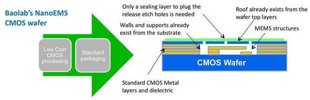
Process Allows Nanoscale MEMS to be created inside CMOS wafer.
NanoEMS(TM) technology enables construction of nanoscale MEMS (Micro Electro Mechanical Systems) within structure of actual CMOS wafer itself using standard, high-volume CMOS lines. Existing metal layers in CMOS wafer are used to form MEMS structure via standard mask techniques, and Inter Metal Dielectric is etched away using vapour HF. Etching uses equipment already available for volume...
Read More »
Benefits of Interfacing Robots & People in the Supply Chain
Learn how robots generate safer operations, more accurate data, and greater flexibility.
Read More »
Trotec Laser Offers Customizable Industrial Laser Marking Solutions for Any Application
Trotec's laser marking solutions provide your company with configurable workstations and intuitive, customizable software. Check out our video to learn more.
Read More »