Vishay Intertechnology to Showcase Leading Vishay Electro-Films Products at 2014 SPIE Photonics West Exhibition
MALVERN, Pa.Ã- – Vishay Intertechnology, Inc. (NYSE: VSH) today announced that it will be showcasing its latest industry-leading Vishay Electro-Films (EFI) solutions at the 2014 SPIE Photonics West Exhibition, taking place from Feb. 4-6 at the Moscone Center in San Francisco. In booth 5618, products on display will include a wide range of Vishay EFI custom submounts, custom substrates with...
Read More »
Thermal Technology Ships 14 K1 Sapphire Crystal Growers to Europe
SANTA ROSA, Calif.-Ã- Thermal Technology, a leading manufacturer of crystal growth equipment and high temperature furnace systems, recently shipped 14 K1 HB LED-grade sapphire crystal growers to a customer in Europe.Ã- The K1’s large 90kg sapphire boule is optimized for 4” and 6” cores used in LED production, with 8” cores possible. “We continue to strengthen our position in...
Read More »HexaTech Validates AlN Substrate Platform for UV-C Laser Fabrication with Record-Breaking Lasing Performance
Lasing breakthrough demonstrated in optically pumped, 264 and 280 nm lasers fabricated on HexaTech AlN substrates MORRISVILLE, N.C. - In a parallel effort to its development of UV-C light emitting diodes (LEDs), HexaTech recently demonstrated optically pumped, AlGaN-based lasers grown on highest-quality, single crystalline AlN substrates. Laser structures fabricated at HexaTech and tested in...
Read More »Ahlstrom Achieves Registered Latex Developer Certification from HP
Ahlstrom Corporation PRESS RELEASE - Ahlstrom Corporation, a global high-performance materials company, has taken part in the HP Registered Latex Development Program and a wide number of Ahlstrom's poster papers and wallcover substrates have met the HP compatibility standard. After successful completion of the certification tests on different large-format HP Latex printers, Ahlstrom has been...
Read More »
Choosing the Right Scrap & Chip Conveyor System
Understanding the different types of scrap and chip conveyors.
Read More »Lead Carrier Substrate enables multi-row QFN packages.
Comprised of sintered metal array of wire bond and die attach pads delivered on temporary thin metal strip, xLC(TM) substrate enables packaging companies to produce Quad Flat No Lead (QFN) semiconductor packages with hundreds of leads and multiple rows. This direct replacement for leadframe is completely compatible with all QFN processing and enables packages to be made with as many rows as...
Read More »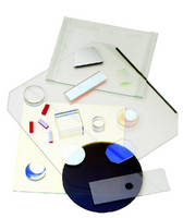
Abrisa Technologies Provides Precision Bio-Tech Glass Fabrication & Thin Film Coatings for Medical Devices
Abrisa Technologies designs, manufactures, and most importantly, delivers customized precision optical glass assemblies and thin film optical coatings for medical devices and analytical instruments. Glass is often the material of choice for medical test devices and analytical instrumentation where material compatibility, durability, and transparency are required. Glass is cleanable, dimensionally...
Read More »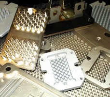
Pin Fin Coolers suit hybrid vehicle IGBT applications.
Coolers with AlSiC (Aluminum Silicon Carbide) metal matrix composite pin fin substrates are designed for liquid-cooled, high-power module systems used in hybrid electric vehicle applications. They provide isotropic thermal expansion (8 ppm/Ã-
Read More »Ceramic Substrate suits thick-film applications.
Designed to address miniaturization and higher-power applications, DuraStrate consists of fine-grained (1.5-2.0 micron) microstructure material optimized for biaxial flexural strength, consistent thicknesses, camber flatness, and aged adhesion. Ceramic substrate material is designed for optimal performance in very thin (10-15 mil) varieties of thick-film substrates.
Read More »PGI Introduces New Moldable Substrates for the Automotive Industry
Recyclable Material for Trunk and Wheel Well Liners Reduces Noise in Vehicles MIAMI, April 26 /- Polymer Group, Inc. (PGI) (OTC Bulletin Board: POLGA; POLGB) today introduced new substrates for moldable automotive components made from recyclable materials that improve acoustics in vehicles. Used in trunk and wheel well liners, the substrates made from recyclable polypropylene and polyethylene...
Read More »Cree Demonstrates 100-mm Zero-Micropipe Silicon Carbide Substrates
DURHAM, N.C., MAY 23, 2007 - Cree, Inc., (Nasdaq: CREE) announced today that it has achieved another milestone in the development of silicon carbide (SiC) technology with the demonstration of 100-mm (4-.in.), Zero-Micropipe (ZMP(TM)), n-type SiC substrates. Micropipes, common crystalline defects in SiC, can not only decrease the number of usable electronic devices produced per wafer, but can also...
Read More »
Basalt America Announces Stronger, Lighter, and Corrosion-Free FRP's (Fiber Reinforced Polymers)
Fiber Reinforced Polymers (FRP), represents a truly groundbreaking advancement in structural reinforcement. Lightweight, strong, and green, they are changing the way the construction industry thinks about rebar. Unlike steel, FRPs don't rust and are far stronger than standard rebar. To learn why Fiber Reinforced Polymers are poised to change the way the world builds, see our video.
Read More »