Copper Barrier-Seed PVD System is intended for TSV packaging.
Share:
Press Release Summary:
For copper barrier-seed applications, INOVA® NExT PVD system features Hollow Cathode Magnetron (HCM) IONX source technology. Copper barrier-seed physical vapor deposition (PVD) process, intended for through-silicon-via (TSV) packaging market, delivers optimal sidewall and bottom coverage and enables void-free copper fill during subsequent TSV electroplating step. TSVs enable 3D packaging, where multiple chips are stacked on top of each other into one 3D module.
Original Press Release:
Novellus Develops Advanced Copper Seed Technology for Through-Silicon-Via (TSV) Packaging
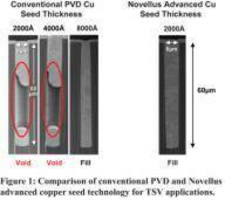
New PVD HCM(R) Process Enables Void-free Copper Fill Of High Aspect Ratio TSV Structures SAN JOSE, Calif. -- Novellus Systems (NASDAQ:NVLS) today announced that it has developed a new, advanced copper barrier-seed physical vapor deposition (PVD) process for the emerging through-silicon-via (TSV) packaging market. The process uses Novellus' production-proven INOVA® platform with patented Hollow Cathode Magnetron (HCM) technology to produce highly-conformal copper seed films that are four times thinner than the conventional PVD seed approaches used for TSV applications. The HCM TSV process delivers excellent sidewall and bottom coverage, and enables void-free copper fill during the subsequent TSV electroplating step. In contrast to the traditional two dimensional, pin-based chip packaging approach, TSVs enable three dimensional packaging, where multiple chips are stacked on top of each other into one space-saving 3-D module. The 3-D stacked chips are connected to each other with short TSV copper interconnects that result in increased device speed and lower power consumption. TSV enabled 3-D packaging delivers the increased functional density and smaller packaging footprint important for today's ever-shrinking mobile consumer electronics. TSV copper interconnects utilize a conventional damascene deposition sequence of PVD copper barrier-seed followed by electrochemical copper fill to create the "pillars" that connect one chip to another. As compared to a traditional, dual damascene copper interconnect scheme, a TSV feature is extremely deep, in some cases up to 200 microns. This high aspect-ratio structure makes the deposition of conformal seed layers very challenging. Non-conformal copper seed layers have minimal sidewall coverage, and can lead to void formation during the subsequent copper TSV fill step, directly impacting device reliability. Conventional TSV integration sequences have addressed this issue in several ways. One method is to "relax" the aspect ratio of the feature by tapering the TSV etch process to create vias with non-vertical sidewalls. While this increases the subsequent PVD step coverage, it limits the ultimate packaging density that can be achieved. Another method is to deposit a thicker copper seed layer to achieve sufficient sidewall coverage within the TSV feature, although this results in an expensive manufacturing process due to higher cost of consumables and lower system throughput. Novellus engineers have developed an HCM-based advanced copper barrier-seed process for TSV applications that addresses both the technical challenges and high manufacturing costs associated with the conventional approaches. The innovative technology uses a patented ring of permanent magnets within the PVD process chamber to create a strong, locally ionized field, which results in an increased ion density on the sidewalls of the TSV structure. Increasing the ion density in this region causes a larger fraction of the sputtered film to land on the sidewall, which in turn results in a more conformal deposition. This highly conformal process eliminates the need for tapered sidewalls and allows the deposited film thickness to be four times thinner than the typical PVD seed layers used for TSV applications. As shown in Figure 1, Novellus' advanced seed process can achieve void-free feature fill in a 60 micron deep, 10:1 aspect ratio TSV feature with vertical sidewalls using a 2000 angstrom thick copper seed layer. The conventional PVD approach requires an 8000 angstrom thick seed layer to achieve the same result. The 4X thinner TSV seed layer results in a substantial increase to system throughput and reduces the cost-of-consumables by greater than 50 percent as compared to conventional PVD approaches. "TSV 3-D technology holds great promise for advanced semiconductor packaging applications, assuming that both the technological and productivity challenges can be addressed," said Dr. Fusen Chen, Novellus' executive vice president of semiconductor systems products. "Novellus' new advanced seed process addresses both of these challenges for the copper barrier-seed portion of the TSV integration sequence, resulting in a thin, highly conformal film with exceptional PVD system throughput to meet the needs of high volume manufacturing." About Novellus' PVD Copper Barrier/Seed Technology: For copper barrier-seed applications, Novellus' INOVA® NExT PVD system features a patented Hollow Cathode Magnetron (HCM) IONX source technology, providing highly conformal barrier films and scalable seed layers that extend PVD technology to the 2x technology node and beyond. About Novellus: Novellus Systems, Inc. (NASDAQ:NVLS) is a leading provider of advanced process equipment for the global semiconductor industry. The company's products deliver value to customers by providing innovative technology backed by trusted productivity. An S&P 500 company, Novellus is headquartered in San Jose, Calif. with subsidiary offices across the globe. For more information, please visit www.novellus.com Novellus, INOVA and HCM are registered trademarks of Novellus Systems, Inc.