

Group4 Labs LLC
Menlo Park, CA 94025
Share:
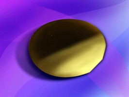
Gallium Nitride-on-Diamond-® Wafer has 2 in. diameter.
GaN-on-diamond semiconductor wafer features single GaN layer atomically attached to freestanding, 25 micron thick, polycrystalline CVD diamond substrate. Nanometer proximity of chip's active region to diamond reduces heat build-up by extricating heat from core at instant of generation, permitting high temperature resilience for high-power, high-frequency electronic, solid-state white lighting,...
Read More »Semiconductor Wafer addresses classic heat problems.
Available in 10 x 10 mm square pieces, GaN-on-diamond Xero Wafer(TM) consists of gallium nitride layer atomically attached to freestanding, polycrystalline chemical-vapor-deposited diamond substrate measuring 25 microns thick. GaN that is exposed offers atomically smooth surface finish that is epi-ready for further epitaxial deposition. Sub-nanometer proximity of chip's active region to diamond...
Read More »