EV Group Ships Temporary Bonding/Debonding System to Fraunhofer ISIT for Developing Advanced Power Devices
EVGÃ-® 850TB/DB product order follows multi-year process development cooperation in thin-wafer applications for PowerMOS and Insulated Gate Bipolar Transistor (IGBT) devices ST. FLORIAN, AustriaÃ- – EV Group (EVG), a leading supplier of wafer bonding and lithography equipment for the MEMS, nanotechnology and semiconductor markets, today announced that the Fraunhofer Institute for...
Read More »QuantumClean-® and ChemTrace-® to Exhibit at SEMICON Korea 2014
Global Leader in Semiconductor High Purity Process Parts Cleaning, Performance Coatings and Microcontamination Analytical Laboratory Services™ to exhibit at SEMICON Korea 2014 tradeshow. QUAKERTOWN, Pa. - QuantumCleanÃ-® and ChemTraceÃ-® today announced that they will be exhibiting at the SEMICON Korea tradeshow, held at the Coex in Seoul, South Korea from February 12(th) through...
Read More »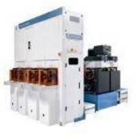
Dielectric Deposition System is designed for 3D chip packaging.
Applied ProducerÃ-® InVia(TM) dielectric deposition system uses CVD process to deposit uniform, thick oxide films in greater than 10:1 high aspect ratio (HAR) through-silicon via (TSV) structures. Process also enables electrical isolation of TSV to ensure reliable performance. For 3D packaging schemes, it electrically connects chips that are vertically stacked to boost speed and lower power...
Read More »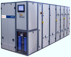
Exhaust Management Systems use vacuum and abatement technologies.
Incorporating iXH harsh process vacuum pump and Atlas(TM) gas abatement solutions, Zenith(TM) series helps address vacuum and abatement demands for advanced semiconductor processing at 60 nm and smaller design rules. It offers range of turnkey, process-centric exhaust management solutions for semiconductor manufacturing. Featuring completely integrated components, product range provides full...
Read More »
5 Common Liquid Injection Molding Mistakes (And How to Avoid Them)
This guide offers insights about steering clear of common LIM problems and maximizing your project's efficiency.
Read More »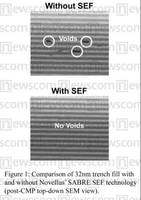
Novellus' Suppression-Enhanced Fill(TM) Technology Provides Defect-Free 32nm Copper Interconnects
Unique Hardware and Process Chemistry Extend Cu Manufacturing Capability SAN JOSE, Calif., April 9 / -- Since the advent of copper damascene processing, achieving void-free fill of high aspect ratio interconnect features has been a key challenge for device manufacturers. Shrinking dimensions at each successive technology node have increased the complexity of the copper seed and electroplating...
Read More »Imprint Lithography Tool meets semiconductor overlay needs.
Leveraging S-FILÃ-® (Step and Flash Imprint Lithography) technology, ImprioÃ-® 300 is used for IC prototyping and process development at 32 nm node and beyond. It offers sub-10 nm resolution patterning in single exposure and can create dense, high-resolution structures in 2 dimensions. Drop-in technology - suitable for mix-and-match strategies where resolution advantage can be deployed on...
Read More »VESTA Announces Multi-Chamber Order for Its VULCAN System to Leading Foundry in Taiwan
Posted: November 27, 2007 VESTA Technology, Inc., a leading supplier of production proven thermal process systems and an industry innovator in atomic layer deposition (ALD), today announced it received a multi-chamber order for its VULCAN(TM) Single wafer High-k and Metal ALD system from the largest leading foundry based in Taiwan. The foundry, a new ALD customer for VESTA, plans to utilize the...
Read More »Data I/O Announces New Generation Flash Technology
REDMOND, Wash., Aug. 1 /-- Data I/O (NASDAQ:DAIO) has today released a new generation of device programming technology that continues the company's leadership position in providing the most advanced programmable device support for Flash memory and microcontroller devices. Known as FlashCORE II, this hardware and software combination significantly extends the company's advanced architectures and...
Read More »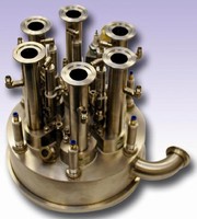
Gas Abatement Solution aids in semiconductor processing.
Based on inward-fired combustion technology, HELIOS 6(TM) gas abatement solution has head design with 6 inlets for process gases and one inlet for gas box purges or other ancillary operations. Unit does not require compressed air and can reduce hydrogen concentrations below lower explosive limit (LEL) in flows as high as 200 slm. Applications include high hydrogen flow processes, such as Si and...
Read More »Nyden Details a Proactive Role in Designing a New Generation of Large-Scale Integration (LSI) Chips for Optimal Speed, Power and Resolution in All Design Areas of Next-Generation Semiconductor Equipment
For Immediate Release: May 23rd, 2007 Nyden Details a Proactive Role in Designing a New Generation of Large-Scale Integration (LSI) Chips for Optimal Speed, Power and Resolution in All Design Areas of Next-Generation Semiconductor Equipment. High-Performance LSI chips for the Semiconductor Manufacturing and Inspection Technology Industries. San Jose, CA--Nyden Corporation and its parent company,...
Read More »
Complete Water Solutions Offers Wide Range of Water Treatment Equipment
Complete Water Solutions provides full installation tailored to your water treatment needs. Check out the video to learn more.
Read More »