The National Physical Laboratory Uses NanoSight NTA System for Nanoparticle Characterization
Salisbury, UK: NanoSight, world-leading manufacturers of unique nanoparticle characterization technology announce that the UK's National Physical Laboratory uses the LM-10 system for their studies in nanoparticle characterization. The National Physical Laboratory routinely looks at emerging techniques to evaluate their performance for the quantitative characterization of nanomaterials....
Read More »NEC Succeeds in Fabrication of CNT Transistor Using Coating Process; Confirms Feasibility of Environmentally Friendly Electronic Devices Using CNTs
Tokyo, Japan, Feb 13, 2008 - NEC Corporation today announced the successful development of a carbon nanotube (CNT) transistor using a coating process. The basic operation of the new transistor with advanced characteristics has been verified, confirming its application in the printed electronics field. Main features of the new CNT transistors (1) Based on an NEC device model, design guidelines...
Read More »University of Tuebingen Ready to Produce Carbon Nanotubes on AIXTRON CVD System
Posted: November 28, 2007 AIXTRON AG announced the installation and commissioning of a Nanoinstruments Black Magic 2-inch R&D equipment for carbon nanotube (CNT) growth at the Physics and Chemistry Research Facility, University of Tuebingen, Germany. The new equipment combines both thermal CVD and plasma enhanced CVD in a single platform, and will be used for the development of carbon...
Read More »First Nano Ships Boron Nitride Nano Tube System to Center for Functional Nanomaterials @ Brookhaven National Laboratory
RONKONKOMA, N.Y., Jan. 10 - First Nano, a division of CVD Equipment Corporation (NASDAQ:CVV), announced today the shipment of an ET3000-BN Chemical Vapor Deposition System to the Center for Functional Nanomaterials (CFN) at Brookhaven National Laboratory (BNL). The ET3000-BN system was configured specifically for Boron Nitride Nanotubes (BNNT's) and is, to the best of our knowledge, the first...
Read More »
Choosing the Optimal IDC & Medical PPE Supplier
This white paper provides an in-depth overview into infectious disease control (IDC) medical PPE including development, key benefits, applications and product offerings.
Read More »Carbon Nanotube Tool Developer Appoints AxR as its US Representative
MRS Fall Exhibit, Boston, MA, November 27, 2007 - Surrey NanoSystems has appointed Axiom Resources Technologies (AxR) as its US representative. The agreement provides local technical support throughout North America for the company's novel low-temperature carbon nanotube growth tool, via AxR's headquarters in Orange, California, and a large network of regional support staff. Surrey NanoSystems'...
Read More »Heidelberg Instruments to Support Nano Research at the University of California, Santa Barbara, Nano Fabrication Facility
Heidelberg, Germany, November 20, 2006 -- Heidelberg Instruments announced the sale of an advanced DWL200 maskless laser lithography system to the Nano Fabrication Facility at the University of California, Santa Barbara. The DWL200 system will enable the user to expose sub micron structures on photoresist, with an active write area of up to 200 mm by 200 mm. About Heidelberg Instruments, GmbH...
Read More »Heidelberg Instruments to Support Micro and Nano Research at the University of Uppsala, Sweden
Heidelberg, Germany, November 23, 2006: Heidelberg Instruments announced the sale of an advanced DWL200 maskless laser lithography system to the Angstrom Microstructure Laboratory of the University of Uppsala, Sweden. The DWL200 system will enable the user to expose sub micron structures on photoresist, with an active write area of up to 200 mm by 200 mm. The DWL 200 lithography system will...
Read More »Nanophase Notes New Order
ROMEOVILLE, Ill., Nov. 6 // -- Nanophase Technologies (NASDAQ:NANX), a technology leader in nanomaterials and advanced nanoengineered products, announced receipt of a new order for polishing nanodispersions for a confidential Asian customer. The Company believes the nanodispersions will be used for LCD screen polishing. As we have stated previously, we are extending our nanomaterials and...
Read More »Imperial College London Unveils UK's First Titan (TM) S/TEM
World's Most Powerful Commercially-Available Microscope Provides Access to Atomic-Scale Data for Nanotechnology Research OCTOBER 18, 2006/Hillsboro, Ore.--Imperial College London has unveiled one of the UK's most powerful microscopes, the Titan(TM) 80-300 S/TEM from FEI. It is the world's most powerful commercially-available scanning/transmission electron microscopes and one of the only...
Read More »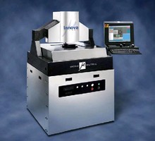
Optical Measurement System uses image analysis algorithms.
Based on sound metrology principles, Innova provides point-to-point and field-of-view non-contact measurements of semiconductor, optoelectronic, and MEMS devices. It delivers FOV measurement down to 0.5 Ã-µm with measurement accuracy of 0.010 Ã-µm. Providing 200 x 200 mm XY stage travel, system has granite structural components and vibration isolation support stand for stability....
Read More »
Solder Redefined
Indium Corporation has developed a new twist on traditional solder by developing a composite with a reinforced matrix internal structure. The result is a solder with increased strength and reliability. Check out this video to learn more about the mechanics behind the groundbreaking technology.
Read More »