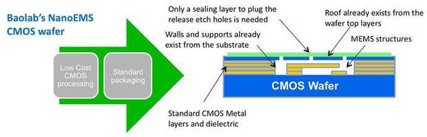
Process Allows Nanoscale MEMS to be created inside CMOS wafer.
NanoEMS(TM) technology enables construction of nanoscale MEMS (Micro Electro Mechanical Systems) within structure of actual CMOS wafer itself using standard, high-volume CMOS lines. Existing metal layers in CMOS wafer are used to form MEMS structure via standard mask techniques, and Inter Metal Dielectric is etched away using vapour HF. Etching uses equipment already available for volume...
Read More »
Specifying Removable Insulation Blankets - A Guide for Engineers
Looking for guidance on how to spec removable insulation? Download our free guide for engineers now!
Read More »
What Can Test Devices Spin for You?
Test Devices helps you ensure the safety and efficiency of your high performance machines with cutting edge spin testing, rotor engineering, and precision balancing capabilities. Check out the video to learn more.
Read More »