Stepper Family suits nanotechnology applications.
NanoTech(TM) 100 offers 1.0 or 0.8 micron lens options, Machine Vision System (MVS), and PC controller. NanoTech 160 is available with 2.0, 1.0, or 0.8 micron lens. NanoTech 190 offers 2.0 or 1.0 micron lens and application-specific, air-bearing rowbar patterning system. Designed for processing thick and thin films, NanoTech 200 features 1.4 or 1.0 micron lens options. With production resolution...
Read More »
Choosing the Optimal IDC & Medical PPE Supplier
This white paper provides an in-depth overview into infectious disease control (IDC) medical PPE including development, key benefits, applications and product offerings.
Read More »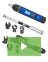
Error Proofing by Design
Sturtevant Richmont's torque tools help customers cut rework and warranty costs while increasing throughput.
Read More »