Heidelberg Instruments, GmbH, Announces the Order of an Advanced Maskless Lithography System by a Major Japanese Based customer
Heidelberg, Germany, November 8, 2006: Heidelberg Instruments, GmbH, Heidelberg, Germany, a leading supplier of direct write laser lithography systems, announced the sale of an advance MW800fbm to a major company in Japan. This system will be used for production of high end display components. MW800fbm is the latest generation of maskless lithography systems supplied by Heidelberg Instruments for...
Read More »SF-100 Rotational Stage Assembly Provides MicroPatterning of Cylindrical Surfaces
St. Petersburg, Florida, October 24, 2006: Intelligent Micro Patterning, LLC, St. Petersburg, Florida, announced a new, unique enhancement to the SF-100 maskless micropatterning system, termed the SF-100 Rotational Stage Assembly. This additional capability allows for micro patterning of features seamlessly on cylindrical curved surfaces. The SF-100 is a unique, maskless photolithography system...
Read More »Ultratech Expands Advanced-Packaging Offerings with New Low-Cost Unity Platform(TM)-Based Tools Targeting Foundry Customers
Unity GOLD and Unity PLATINUM Deliver Low-risk, Low-cost, Production-Proven Lithography Solutions SAN JOSE, Calif., Sept. 19 /-- Ultratech, Inc. (NASDAQ:UTEK), a leading supplier of lithography and laser-processing systems used to manufacture semiconductors and nanotechnology devices, today introduced two new advanced-packaging (AP) lithography tools built on the company's highly successful Unity...
Read More »Heidelberg Instruments to Support MEMS Research at the Institute of Electron Technology, Poland, with an Advanced DWL200 Maskless Laser Lithography System
2006-09-16--Heidelberg, Germany, September 16, 2006: Heidelberg Instruments announced the sale of an advanced DWL200 maskless laser lithography system to the Institute of Electron Technology Warsaw, Poland. The DWL200 system will enable the user to expose minimum structures on photoresist down to 0.6 microns, with an active write area of up to 200 mm by 200 mm. The DWL200 maskless lithography...
Read More »
PCB Fabrication Notes Guide
The overall purpose of your fabrication notes is to enhance Design for Manufacturability for optimal PCB fabrication and assembly while maintaining applicable industry standards and regulations.
Read More »Heidelberg Instruments to Support Micro and Nano Research at the Boston University Photonics Center, Boston, USA
Heidelberg, Germany, September 13, 2006: Heidelberg Instruments announced the sale of an advanced DWL66 fs maskless laser lithography system to the Boston University Photonics Center. The DWL66 fs maskless lithography system is capable of binary and gray scale exposure, layer to layer alignment, and is able to produce minimum features down to 0.6 microns. The Heidelberg direct write laser system...
Read More »Intelligent Micro Patterning Provides SF-100 to Purdue University for Development of Three Dimensional MicroScale Rapid Prototyping
Intelligent Micro Patterning Provides SF-100 to Purdue University for Development of Three Dimensional MicroScale Rapid Prototyping St. Petersburg, Florida, April 5, 2006: Intelligent Micro Patterning, LLC, St. Petersburg, Florida, announced the sale of an SF-100 maskless exposure system to the Department of Electronic and Electrical Engineering at Purdue University, West Lafayette, Indiana. The...
Read More »Analyzer facilitates lithography cell qualification.
Integrated with Archer overlay, eCD CD SEM, and SpectraCD optical CD metrology platforms for 65 nm and below IC production, K-T Analyzer lithography correctable platform provides automated, on-tool analysis of overlay and critical dimension metrology data in real time. System gives engineers immediate feedback on quality of lithography process, enabling them to correct errors, minimize...
Read More »Luminescent to Provide Enabling Lithography Platform to Cypress's Silicon Valley Technology Center
SVTC and Luminescent to Jointly Develop New Manufacturing Approach Using Inverse Lithography Technology (ILT) MOUNTAIN VIEW, Calif. and SAN JOSE, Calif., Oct. 3 -- Luminescent Technologies, Inc. and Silicon Valley Technology Center (SVTC), a division of Cypress Semiconductor Corp. (NYSE:CY) today announced a joint development program in which the companies will collaborate on advanced lithography...
Read More »Chip Mask Creator provides complete ILT capability.
Acting as replacement for Resolution Enhancement Technology (RET) software, Explorer uses Inverse Lithography Technology (ILT) platform to evaluate desired on-wafer pattern and mathematically determine mask features needed to produce intended silicon outcome. ILT analyzes entire image and generates globally optimized mask design in single pass. Combining software and hardware, Explorer features...
Read More »
AFM System offers nanolithography and manipulation feature.
MFP-3DÃ-® AFM System consists of digital controller, Igor Pro software, and Nanopositioning system. With MicroAngelo feature, system allows nanolithography images to be imported from other programs or generated within software environment. Imported images are converted into series of contour lines which are then scaled and used to drive scanner to create lithographic image. Sensored, closed...
Read More »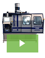
New Davenport Hybrid Machine Offers Unique Flexibility for Parts Manufacturing
The Davenport Hybrid machine offers greater flexibility, easier set-ups, and faster cycle times. Check out the video to learn more.
Read More »