x x.
Share:
Press Release Summary:
x
Original Press Release:
Jenoptik's Optical Systems Division with New Developments at LASER in Munich
At the LASER World of Photonics from May 23rd to 26th, 2011 the Optical Systems Division of Jenoptik will be demonstrating new F-Theta Lenses for high-power laser applications, its capabilities for the fabrication of non-rotationally symmetric optical surfaces in the sub-µm range and a new generation of LED Point Source Dies. The presentation will also feature the specific ranges of services offered by the Division's Business Units: Optics, Microoptics and Optoelectronic Systems.
Further information about the exhibition program of Jenoptik's Optical
Systems Division is also available at: jenoptik.com/laser2011.
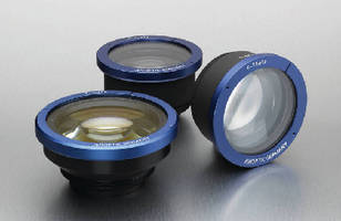
New F-Theta Fused-Silica Lenses for Laser Material Processing
Fiber lasers and other types of lasers will output increasing laser power, therefore the requirements on equipment for laser material processing are becoming more stringent.
The Optics Business Unit makes its first presentation of a new series of Fused-Silica F-Theta Lenses that work at wavelengths of 266 nm and 355 nm. These lenses combine the benefits of standard F-Theta lenses, yet also provide a distinctly higher damage threshold.
Especially the new 355 nm F-Theta Lens provides optimized performance in high-power laser applications. Of diffraction-limited design, the lens features high spot uniformity over the entire scan range. Its coatings which have been specifically optimized for fused-silica optics warrant low absorption.
Two more F-Theta Fused-Silica Lenses will be available for operation at the wavelength of 1070 nm and with different focal lengths (f = 160 nm and f = 255 nm) beginning in the fourth quarter of 2011.
These diffraction-limited objective lenses are intended for laser powers up to 2 kW at 1070 nm. An additional choice of F-Theta Fused-Silica Lenses is planned for use at different wavelengths in the UV, VIS and NIR ranges to complement the Unit's range of products.
The Optics Business Unit is a competent partner in the field of integrated optical modules and systems. Jenoptik offers innovative optical solutions with special focus on laser material processing - from the formation of an intensity beam profile to the splitting of high-intensity laser beams.
At the LASER World of Photonics, Jenoptik will demonstrate, by way of a sample application, its competence in optical modules for laser material processing - from the point of coupling a laser beam into a fiber to the stages of beam expansion and beam splitting with the help of a specifically adapted diffractive component and onto focusing performed by the F-Theta Lens.
Fabrication of Non-Rotationally Symmetric Optical Surfaces Now also in the Sub-ìm Range
The Optoelectronic Systems Business Unit is now able to offer its customers services to fabricate optical free-form surfaces, including with accuracies in the sub-µm range.
Smaller, lighter and more compact - miniaturized optics with free-form surfaces unite the functionalities of multiple optical components "within the narrowest of space" thus providing a variety of functions. Optical free-form surfaces are required wherever a complex distribution of light or light density has to be achieved, for example, in HUDs (Head-Up Displays) for vehicles and airplane cockpits or also HMDs (Head-Mounted Displays) and video eyeglasses.
Using Slow-Tool Servo* Technology combined with monocrystalline diamond instruments, Jenoptik manufactures injection molding tools for non-rotationally symmetric surfaces with an accuracy smaller than 0.5 µm. This tool manufacturing technology makes it possible to produce highly precise polymer optics in an injection-molding process. Jenoptik maintains a stable environment in air-conditioned, vibration-isolated manufacturing facilities as necessary to perform ultra-precision machining on CNC machinery that represents state of the art, supported by advanced metrology
equipment and measuring techniques.
The Jenoptik Optoelectronic Systems Business Unit is an expert in everything that relates to the manufacture of optics by way of injection molding - from prototyping to the injection mold and onto the various optical polymer components and optoelectronic systems with free-form surfaces.
Under a BMBF-funded project Jenoptik is joining forces with partners in science and industry to work on the complex issue of free-form technology in an effort to master the highly precise shaping of free-form surfaces.
New Generation of LED Point Source Dies Emits Red Light
Innovative materials and extended technologies make LED point source dies perform even more efficiently in terms of power and current consumption. LED point source dies generate a circular emission area that can easily be imaged and focused. With the new point source dies, emission at 650 nm can already be perceived beginning at an approximate size of 400 nA.
Compared to the previous generation, the new point source dies generate a 5 times higher luminous intensity. The high efficiency results in extended battery life which makes it interesting for portable applications. The high current capacity up to 500 A/cm² and the very low switching times predestine these point sources for data transfer applications. Furthermore, LED point source dies can be relied on to function for a lifetime as long as 100,000 h at 100 A/cm².
Jenoptik offers LED point source dies in standard versions (see illustration below) and customized versions of different shape and spot diameters variable up to 200 ìm. They can be used e. g. for replacement of VCSEL semiconductor lasers (no formation of speckle patterns), as radiation source for rotation transducer sensors, as miniature light point in optical sights, as focused beam for light barriers and in dot-line arrays for printers.
To form your own opinion about the many applications and potential uses of our products from Optics, Microoptics and Optoelectronic Systems, come and visit us in hall C2, booth # 411.
About Jenoptik Optical Systems division
With its Optical Systems division, the Jenoptik Group is one of the few manufacturers in the world to produce precision optics and systems designed to meet the highest quality standards.
Besides opto-mechanical and opto-electronical systems, modules and assemblies, the Optical Systems division is a development and production partner for optical, microoptical and coated optical components - made of optical glasses, IR materials as well as polymers. It possesses outstanding expertise in the development and manufacture of optics and microoptics for beam shaping used in the semiconductor industry and laser material processing.
The product portfolio also includes systems and components for life sciences as well as automotive, lighting and machine vision applications, for digital image capture and processing as well as cameras for digital microscopy.
Contact
Dr. Markus Besenbeck
Director Marketing & Business Development
JENOPTIK Optical Systems GmbH
Goeschwitzer Strasse 25
07745 Jena I Germany
Phone: +49 3641 65-2276 I Fax -3658
info.os@jenoptik.com
www.jenoptik.com/os