Wafer Bonding Systems support wafers up to 200 mm in diameter.
Press Release Summary:
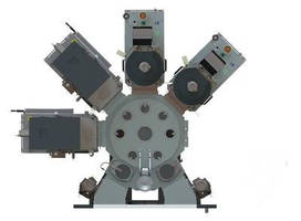
Designed for universities and R&D groups, EVG®580 ComBond® System comes with 1 cassette station or manual load port as well as single-arm robot, supporting up to 3 process modules. EVG580 ComBond HVM, intended for high-volume manufacturing, can be configured with 2 cassette stations or equipment front-end module with up to 4 cassettes for continuous operation. System comes with dual-arm robot to support up to 6 process modules for max throughput. Both operate in high-vacuum-process environment.
Original Press Release:
EV Group Extends Leadership in High-Vacuum Wafer Bonding Technology
Two new EVG®580 ComBond® system configurations address university / research & development and high-volume manufacturing needs respectively
ST. FLORIAN, Austria -- EV Group (EVG), a leading supplier of wafer bonding and lithography equipment for the MEMS, nanotechnology and semiconductor markets, today introduced two new configurations to its EVG(®)580 ComBond(®) series of automated high-vacuum covalent wafer bonding systems. Addressing the needs of universities and R&D institutes, and high-volume manufacturing (HVM) requirements, respectively, both system configurations achieve electrically conductive and oxide-free bonds of materials with different lattice constants and coefficients of thermal expansion at room temperature.
Applications that demand room-temperature bonding of substrates with very different material properties and that are supported by the EVG580 ComBond series include advanced engineered substrates, power devices, stacked solar cells and emerging technologies such as silicon photonics.
New Configuration Details
The new entry-level EVG580 ComBond system for universities and R&D institutes comes with one cassette station or manual load port as well as a single-arm robot, supporting up to three process modules. The EVG580 ComBond HVM system can be configured with two cassette stations or an equipment front-end module with up to four cassettes for continuous mode operation, as well as comes with a dual-arm robot to support up to six process modules for maximum throughput.
Both new ComBond system configurations, as well as the standard system that can accommodate up to five process modules, are built on a modular platform supporting wafers up to 200 mm in diameter. In addition to one or more bond chambers, the systems feature a dedicated ComBond Activation Module (CAM), which provides advanced surface preparation by directing energized particles to the substrate surface to achieve a contamination-free and oxide-free bond interface. The systems operate in a high-vacuum-process environment with base pressures in the range of 5x10(-8) mbar, which prevents re-oxidation of the treated wafers prior to the bonding step.
"The EVG580 ComBond system with its standard five-module configuration, which was launched last autumn, has already demonstrated its capabilities with multiple R&D partners and customers," stated Dr. Thomas Glinsner, corporate product management director at EV Group. "With the new three-module system, we will now make this breakthrough technology available to universities and smaller R&D institutes, which often are at the forefront of pioneering advanced electronic materials and device research, such as heterogeneous integration of compound semiconductors for silicon photonics and other leading-edge applications. All ComBond systems can be further customized to address specific application development needs, such as with special metrology modules utilizing free ports of the high-vacuum handling."
Combining materials with different properties to produce electronic devices can lead to enhanced device performance due to higher carrier mobility as well as open up new capabilities such as the emission of light through silicon, which can enable optical interconnects and routers. However, combining these materials through traditional epitaxial growth processes leads to crystal dislocation defects due to differences in lattice constant and coefficient of thermal expansion, which in turn degrade performance. These issues can be mitigated by growing each semiconductor material separately on optimized growth substrates and then combining them through wafer bonding. Room-temperature covalent bonding is an ideal choice since it eliminates the need for annealing processes, which generate high temperatures that add additional stress due to CTE mismatch. However, a key limitation of room-temperature covalent bonding has been the inability to maintain tight control of the thickness and uniformity of the bond interface layer, including effective removal of particle contaminants and the native oxide layers, which is necessary in order to achieve an interface that has both sufficient bond strength and electrical conductivity between the bonded materials. The EVG580 ComBond addresses these limitations.
About EV Group (EVG)
EV Group (EVG) is a leading supplier of equipment and process solutions for the manufacture of semiconductors, microelectromechanical systems (MEMS), compound semiconductors, power devices and nanotechnology devices. Key products include wafer bonding, thin-wafer processing, lithography/nanoimprint lithography (NIL) and metrology equipment, as well as photoresist coaters, cleaners and inspection systems. Founded in 1980, EV Group services and supports an elaborate network of global customers and partners all over the world. More information about EVG is available at www.EVGroup.com.
CONTACT:
Clemens Schütte
Director, Marketing and Communications
EV Group
Tel: +43 7712 5311 0
E-mail: Marketing@EVGroup.com