Wafer Analysis System quickly diagnoses root cause of defects.
Press Release Summary:
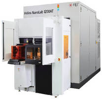
With automated front opening universal pod, Helios NanoLab™ 1200AT DualBeam™ System can be located inside semiconductor wafer lab, where SEM imaging and focused ion beam milling are used to extract ultrathin samples of targeted structures for examination in TEM. System can create site-specific TEM samples thin enough to capture single transistor at 10 nm node, from wafers up to 300 mm in diameter. By moving 1200AT close to wafer process line, process development and ramp are accelerated.
Original Press Release:
FEI Helios 1200AT DualBeam System Accelerates Process Development and Ramp
Full-wafer, near-line analysis delivers results 3X faster than laboratory analysis of cleaved wafers.
Hillsboro, Ore. —FEI (NASDAQ: FEIC) today released the Helios NanoLab™ 1200AT, the newest generation of its full-wafer DualBeam™ analysis systems. The addition of an optional automated FOUP (front opening universal pod) loader allows location of the Helios NanoLab 1200AT system inside the semiconductor wafer fab, where its scanning electron microscope (SEM) imaging and precise focused ion beam (FIB) milling are used by engineers to extract ultrathin samples of targeted structures and defects for examination in a high-resolution transmission electron microscope (TEM).
The results are used to diagnose the root causes of defects and evaluate process maturity. Moving the 1200AT inside the fab and closer to the wafer process line (near-line) can deliver this critical information up to three times faster than laboratory-based analysis of cleaved wafer pieces, enabling acceleration of the development of new processes and the yield ramp to high-volume production.
“The demand for TEM imaging has grown rapidly as semiconductor devices have become too small to be seen with SEM,” said Rudy Kellner, vice president of FEI's Industry Group. “Preparation of the ultrathin samples required by TEM is the rate-limiting step in this analysis. By adding a FOUP loader and moving the Helios NanoLab 1200AT near-line, we can deliver first results many times faster than the hours or days typical when working with wafer pieces in a laboratory outside the fab. Organizationally, there is an advantage if the tool is owned by the same people who need the data. Ultimately, the faster the engineers get results, the faster they can work on debugging and developing new processes to get new products to market.”
The Helios NanoLab 1200AT can create site-specific TEM samples thin enough to capture a single transistor at the 10nm node, from wafers up to 300mm in diameter. In addition to the automatic FOUP loader (AFL), the system takes full advantage of FEI’s recent advances in DualBeam technology.
FEI’s iFast™ automation software now combines wafer, defect- and cell-level navigation with recipe definition and execution in a single, fully-integrated program, ensuring ease-of-use and consistency among operators with varying levels of expertise. The integrated EasyLift™ micromanipulator and QuickFlip™ grid holders support FEI’s process for creating ultrathin TEM samples. The MultiChem™ gas delivery system allows precise control of beam chemistry for fast, selective etching and deposition of protective coatings. An optional low kV STEM detector has been enhanced to provide improved materials contrast, which allows full defect root cause analysis within the fab on a single system.
For more information about the Helios NanoLab 1200AT with AFL DualBeam system, please visit www.fei.com/helios or contact your local sales representative.
About FEI
FEI (Nasdaq: FEIC) is a leading supplier of scientific instruments for nano-scale applications and solutions for industry and science. With more than 60 years of technological innovation and leadership, FEI has set the performance standard in transmission electron microscopes (TEM), scanning electron microscopes (SEM) and DualBeams™, which combine a SEM with a focused ion beam (FIB). FEI has over 2,500 employees and sales and service operations in more than 50 countries around the world. More information can be found at: www.fei.com.