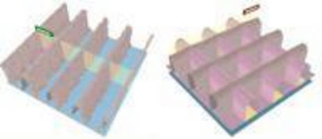
Virtual Lithography Tool addresses EUV and DPL challenges.
Press Release Summary:

PROLITH(TM) X3.1 lets researchers troubleshoot issues in EUV and double patterning lithography (DPL) processes, including line edge roughness (LER) and patterning issues associated with wafer topography. First-principle physics help investigate and optimize lithography processes by simulating patterning results. While stochastic model takes into account quantum behavior of light and discrete reactant molecules in resist, photoelectron model simulates outcome of EUV lithography processes.
Original Press Release:
KLA-Tencor Launches the PROLITH(TM) X3.1 Virtual Lithography Tool for Cost-Effective Investigation of EUV and Double Patterning Lithography Challenges
- Enables increased depth and breadth of lithography research - Helps decrease lithography cell operating expenses - Reduces time required to identify workable lithography solutions
MILPITAS, Calif. -- Today KLA-Tencor Corporation (NASDAQ:KLAC), the world's leading supplier of process control and yield management solutions for the semiconductor and related industries, introduced the latest generation of their PROLITH virtual lithography tool. PROLITH X3.1 enables researchers at leading-edge chipmakers, consortia and equipment makers to quickly and cost-effectively troubleshoot challenging issues in EUV and double patterning lithography (DPL) processes, including line edge roughness (LER) and patterning issues associated with wafer topography. Using PROLITH X3.1 lithographers can streamline their research, conserve valuable lithography cell resources and accelerate product development.
"Researchers face an enormously complex task in evaluating the multiple lithography technologies for the 2Xnm and below design nodes," stated Ed Charrier, vice president and general manager of KLA-Tencor's Process Control Information Division. "They must understand how the pattern printed on the wafer is affected by process-design interactions, including effects of mask designs, scanner settings, wafer topography and variations in resist composition. PROLITH X3.1 uses first-principle physics to help researchers investigate and optimize advanced lithography processes by simulating patterning results rather than printing test wafers. Version X3.1's new EUV and LER models produce accurate results in just a few minutes - making it possible to dramatically reduce product development time. Moreover, this strategy can decrease the amount of scanner, track and CD-SEM tool time diverted to running feasibility experiments, freeing the EUV cell for integration and testing or the optical lithography cell for additional production runs."
PROLITH X3.1 includes several features designed to allow researchers to cost-effectively study different lithography technologies:
-- The first commercially available stochastic model that takes into account the quantum behavior of light and the discrete reactant molecules in the resist, helping researchers to:
- Accurately model LER with a run time of a few minutes, making it practical to study the impact of various process conditions on LER in a real fab;
- Investigate pattern printing repeatability and study the impact on yield;
- Predict line and contact hole CD uniformity;
- Determine the usable process window; and
- Examine how different resist reactant loading levels affect printing (e.g., process windows, CD control, defect levels), allowing material manufacturers to explore resist formulations at significantly reduced cost;
-- The first commercially available photoelectron model that simulates the outcome of EUV lithography processes;
-- Intuitive wafer topography set-up and improved wafer topography models that allow for fast, easy evaluation of double and single patterning non-planar lithography stacks, and next-generation non-planar devices like FinFETs;
-- Database of over 60 high-accuracy, calibrated resist models, available for immediate use;
-- Intuitive interface that runs on a 32-bit PC, capable of providing fast, accurate lithography models without the need for computer upgrades or supercomputers; and
-- Available as an upgrade to the industry-leading PROLITH platform, providing extendibility to protect researchers' existing capital investments.
PROLITH X3.1 is the latest in KLA-Tencor's comprehensive toolset that addresses advanced lithography challenges. For more information on how the PROLITH X3.1 virtual lithography tool can help researchers cost-effectively evaluate advanced lithography technologies, please visit the product web page at: www.kla-tencor.com/lithography-modeling/chip-prolith.html.
About KLA-Tencor:
KLA-Tencor Corporation (NASDAQ:KLAC), a leading provider of process control and yield management solutions, partners with customers around the world to develop state-of-the-art inspection and metrology technologies. These technologies serve the semiconductor, data storage, compound semiconductor, photovoltaic, and other related nanoelectronics industries. With a portfolio of industry-standard products and a team of world-class engineers and scientists, the company has created superior solutions for its customers for over 30 years. Headquartered in Milpitas, California, KLA-Tencor has dedicated customer operations and service centers around the world. Additional information may be found at www.kla-tencor.com. (KLAC-P)


