TI Enters JESD204B Market with Industry's Fastest Dual, 16-Bit ADC and First Clock Jitter Cleaner
ADC provides highest dynamic performance to maximize receiver sensitivity
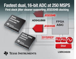
DALLAS - Texas Instruments Incorporated (TI) (NASDAQ: TXN) introduced a pair of devices today supporting the JEDEC JESD204B serial interface standard for data converters. The ADS42JB69 is the industry's first dual-channel, 16-bit analog-to-digital converter (ADC) featuring the JESD204B interface and is also the fastest at 250 MSPS. The LMK04828 is the industry's highest-performance clock jitter cleaner and is the first to support JESD204B clocking. When used together, the devices provide unmatched system-level performance for high-speed systems. For designs requiring a traditional parallel interface, the company also introduced the ADS42LB69, the industry's fastest dual, 16-bit ADC at 250 MSPS featuring an LVDS interface. For more information and to request samples, visit www.ti.com/jesd204b-pr.
JESD204B is an industry-standard serial communications link that simplifies the digital data interface between data converters and other devices, such as FPGAs, DSPs and ASICs. The standard reduces the routing between devices, slashing input/output and board space requirements for applications, such as wireless communications, test and measurement, and defense and aerospace.
The ADS42JB69 maximizes flexibility in system design, because it is the only 16-bit ADC incorporating all three JESD204B subclasses, 0, 1 and 2, allowing multi-device synchronization between data converters. The ADS42JB69 also supports the new JESD204B standard for deterministic latency, which provides fixed transmission delay with or without the use of an external timing signal. The device is also compatible with the existing JESD204A standard.
Key features and benefits of the ADS42JB69 and ADS42LB69
· Highest dynamic performance to maximize receiver sensitivity: At 170 MHz
intermediate frequency (IF), both ADCs provide spurious-free dynamic
range (SFDR) performance of 89 dBc, up to 9-dB better than the
competition, along with SFDR of 100 dBc, excluding harmonic distortion 2
(HD2) and HD3, signal-to-noise ratio (SNR) performance of up to 74.9
decibels relative to full scale (dBFS) and channel isolation of 100 dB.
· Maximum design flexibility with three digital interface choices:
- ADS42JB69 with JESD204B interface reduces the required number of
data interface lanes from 17 to five, slashing board space while
reducing design complexity.
- ADS42LB69 supports traditional parallel interface designs via 17
lanes of double data rate (DDR) low-voltage differential signaling
(LVDS) or 10 lanes of quad data rate LVDS.
· Easy analog input interface: High-impedance analog input buffer with
programmable full-scale range simplifies input filter design and drive
circuitry. This also increases performance uniformity and
device-to-device repeatability across the analog input frequency range.
· Lowest power consumption: The ADS42JB69 consumes 775 mW/channel, while
the ADS42LB69 uses only 740 mW/channel.
· Pin-compatible family for design flexibility: The new ADCs are part of a
family that includes pin-compatible, high-performance 14-bit options.
The dual, 14-bit, 250-MSPS ADS42JB49 (JESD204B) and ADS42LB49 (LVDS)
provide SFDR performance of 89 dBc and SNR performance of up to 73.4
dBFS at 170 MHz IF.
Combining the 16-bit ADS42JB69 with the LMK04828 provides an elegant and simple way for system designers to achieve JESD204B serial interface compliance with reduced bill of materials (BOM), along with unsurpassed performance. The LMK04828 provides ultra-low-jitter and phase noise, while generating the JESD204B subclass 1 system timing reference signal (SYSREF) required for multi-device synchronization.
Key features and benefits of the LMK04828
· Highest performance: Enables less than 100-fs RMS jitter (10 kHz to 20
MHz) at 245.76 MHz using a low-noise voltage-controlled crystal
oscillator module.
· Unique combination of performance and functional integration: Reduces
clock architecture complexity while providing options to maximize system
performance and reduce component count and bill of material (BOM) costs.
· Generates JESD204B subclass 1 SYSREF: High-speed clocks are paired with
JESD204B SYSREF companion signals to provide timing synchronization for
up to seven subsystem JESD204B components.
· Greater flexibility:
- Dual voltage-controlled oscillator cores operating at 2.5 GHz or 2.9
GHz enable maximum flexibility by providing seven pairs of
programmable clock outputs set as LVDS, low-voltage
positive-emitter-coupled logic (LVPECL), or high-swing differential
signaling (HSDS) output formats.
- Output pairs can be configured as a device clock and SYSREF, or as
two device clocks for implementing additional high-speed clocks to
meet system requirements.
- Programmable features, such as digital delay, analog delay and zero
delay, support a variety of clocking requirements and architectures.
Tools and support
The following evaluation modules (EVMs) are available to speed development with the new 16- and 14-bit, 250 MSPS ADCs:
- 16-bit ADS42JB69SEK and 14-bit ADS42JB49SEK with JESD204B interface for
US$999
- 16-bit ADS42LB69EVM and 14-bit ADS42LB49EVM with LVDS interface for
US$399
The EVMs connect to the TSW1400EVM High-Speed Data Capture and Pattern Generation Platform for data analysis, as well as FPGA development platforms from Altera and Xilinx. IBIS models for the ADS42LB69 and ADS42LB49 are also available to verify board signal integrity requirements.
The LMK04828EVAL evaluation module can be purchased today for US$499. The Clock Design Tooland CodeLoader software offer product selection, design and simulation of timing solutions.
Support is available on the High Speed Data Converters and the Clocks & Timers Forums in the TI E2E(TM) Community, where engineers can ask questions and get answers from TI experts.
Availability, packaging and pricing
Samples of the 16-bit ADS42JB69 (JESD204B) and ADS42LB69 (LVDS), and 14-bit ADS42JB49 (JESD204B) and ADS42LB49 (LVDS) are all available today in a 9-mm by 9-mm QFN package. Production quantities are expected in 2Q 2013 with 1,000-unit budgetary pricing of US$185 for the ADS42JB69 and ADS42LB69 and US$125 for the ADS42JB49 and ADS42LB49.
Samples of the LMK04828 are available today in a 9-mm by 9-mm QFN package. Production quantities will be available in 1Q 2013 for a suggested retail price of US$11.20 in 1,000-unit quantities. For systems requiring VCOs operating at 1.9 GHz or 2.5 GHz, the LMK04826 will be sampling in early 1Q 2013 with production quantities available later in the quarter for US$11.20 in 1,000-unit quantities.
Learn more about TI's data converter and clock portfolios by visiting the links below:
- Request samples, purchase EVMs: www.ti.com/jesd204b-pr.
- Download the ADS42JB69 and ADS42JB49 data sheet:
www.ti.com/ads42jb69-pr.
- Download the LMK04828 and LMK04826 data sheet: www.ti.com/lmk04828-pr.
- Download the ADS42LB69 and ADS42LB49 data sheet:
www.ti.com/ads42lb69-pr.
- See how the ADCs and clock can benefit your system in this video:
www.ti.com/jesd204bv-pr.
About Texas Instruments
Texas Instruments semiconductor innovations help 90,000 customers unlock the possibilities of the world as it could be - smarter, safer, greener, healthier and more fun. Our commitment to building a better future is ingrained in everything we do - from the responsible manufacturing of our semiconductors, to caring for our employees, to giving back inside our communities. This is just the beginning of our story. Learn more at www.ti.com.
Trademarks
TI E2E is a trademark of Texas Instruments. All other trademarks and registered trademarks belong to their respective owners.
TXN-P
SOURCE
Texas Instruments Incorporated
CONTACT: Kristina Arnold, Texas Instruments, +1-214-567-8480, karnold@ti.com; or Vicky Smithee, GolinHarris, +1-972-341-2537, vsmithee@golinharris.com
Web Site: www.ti.com