Rudolph Wins Multiple Orders for AWX Unpatterned Wafer Inspection Tools in Back-End and Advanced Packaging Applications
AWX system combines the sensitivity, speed and data analysis needed to optimize back-end processes and minimize cost
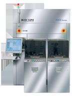
Flanders, New Jersey — Rudolph Technologies, Inc. (NASDAQ: RTEC) announced today that it has won orders for its AWX™ FSI unpatterned wafer inspection system at both a major Southeast Asia-based outsourced assembly and test (OSAT) facility and a key Korean memory manufacturer. In both cases, the systems were selected after direct comparison with entrenched competitors. The AWX FSI inspection system is specifically designed to meet the needs of advanced packaging processes, such as TSV (through silicon via), and other back-end processes. One system shipped in the third quarter and the second will ship in the fourth quarter of 2013.
“Many of the processes being brought into back-end and advanced packaging are similar to those used in the front-end of semiconductor manufacturing, however, the back-end of the line has its own specific requirements and cost of ownership thresholds,” commented Rudolph’s product manager, Reza Asgari. “While it was tempting to simply adopt equipment from the front-end, many of these processes have now evolved to the point that they require systems specifically-designed for the applications and the back-end environment to achieve optimal performance. Our AWX system combines the sensitivity, throughput, handling and data analysis that manufacturers need to optimize their processes and reduce cost.”
Rudolph’s AWX FSI system is a fully-automatic inspection tool for detecting particles, scratches, area defect and micro-roughness (haze) on unpatterned wafers. These systems can be configured in a range of sensitivity/throughput combinations, offering throughputs greater than 120 wafers per hour. The automated handling of different open cassette types and a pre-aligner allows flexibility for using this tool in various environments with a range of wafer types and sizes. Sophisticated software analyzes and reports particles, scratches and haze, and enables automatic wafer sorting based on the inspection results.
For more information about Rudolph’s AWX FSI inspection systems, please visit www.rudolphtech.com.
About Rudolph Technologies
Rudolph Technologies, Inc. is a worldwide leader in the design, development, manufacture and support of defect inspection, advanced packaging lithography, process control metrology, and data analysis systems and software used by semiconductor device manufacturers worldwide. Rudolph provides a full-fab solution through its families of proprietary products that provide critical yield-enhancing information, enabling microelectronic device manufacturers to drive down the costs and time to market of their products. The Company’s expanding portfolio of equipment and software solutions is used in both the wafer processing and final manufacturing of ICs, and in adjacent markets such as FPD, LED and Solar. Headquartered in Flanders, New Jersey, Rudolph supports its customers with a worldwide sales and service organization. Additional information can be found on the Company’s website at www.rudolphtech.com.
Contacts:
Trade Press:
Amy Pauling
952.259.1794
amy.pauling@rudolphtech.com