Rudolph Technologies Announces Rapid Adoption of the Dragonfly G2 System for Advanced Packaging Inspection
One quarter after release, the new Dragonfly platform achieves market recognition in advanced macro inspection with multiple deliveries to world’s largest OSAT
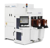
Wilmington, Mass. (January 8, 2019)—Rudolph Technologies, Inc. (NYSE: RTEC) announced today that it has received orders for 12 of its Dragonfly™ G2 system, just months after releasing the product. Several systems were delivered in the fourth quarter to the largest OSAT where the Dragonfly G2 systems displaced incumbent 3D technology and retained the Company’s market leadership in 2D macro inspection. The remaining systems will ship in the first half of 2019 to OSAT, IDM, and Foundry customers who are adopting the Dragonfly G2 platform for its high productivity in two-dimensional (2D) inspection, and its accuracy and repeatability in three-dimensional (3D) inspection of the smallest copper pillars. The Company expects additional adoptions of the Dragonfly G2 system across multiple key market segments in the first half of 2019, which validates Rudolph’s collaborative R&D approach with its key customers.
The new Dragonfly G2 platform delivers up to 150% improvement in productivity over legacy systems as well as exceeds competitive system throughputs. Its modular architecture provides a flexible platform with plug-and-play configurability to combine 2D with 3D Truebump™ Technology for accurate copper pillar/bump height measurements. Clearfind™ Technology detects non-visual residue defects and advanced sensor technology measures 3D features and CD metrology. Additionally, the Dragonfly G2 platform has been specifically architected to allow the measurement, data collection, and analysis of bump interconnects nearing 100 million bumps per wafer using Rudolph’s Discover® software and advanced computing architecture.
“We are pleased that our leading-edge customers across multiple market segments are quickly recognizing the value of the Dragonfly G2 system,” said Michael Plisinski, chief executive officer at Rudolph. “Today’s interconnects for advanced memory are now at or below five microns, which require higher accuracy and repeatability versus standard copper pillar bumps. With approximately 65 wafer-level packages in today’s high-end smartphones, a single weak interconnect or reliability failure can result in a high cost of return, driving our customers’ need for the enhanced process control performance. Defect sensitivity, resolution, and productivity are combined in the Dragonfly G2 system to deliver a capability and cost of ownership that is unparalleled in the competitive space.”
For more information about Rudolph’s process control solutions, visit www.rudolphtech.com.
About Rudolph Technologies
Rudolph Technologies, Inc. is a leader in the design, development, manufacture and support of defect inspection, lithography, process control metrology, and process control software used by semiconductor and advanced packaging device manufacturers worldwide. Rudolph delivers comprehensive solutions throughout the fab with its families of proprietary products that provide critical yield-enhancing information, enabling microelectronic device manufacturers to drive down costs and time to market of their devices. Headquartered in Wilmington, Massachusetts, Rudolph supports its customers with a worldwide sales and service organization. Additional information can be found on the Company’s website at www.rudolphtech.com.
Contacts:
Investors:
Michael Sheaffer
978.253.6273
Trade Press:
Amy Shay
952-259-1794