Rudolph JetStep Lithography System Selected for First Panel Fan-out Packaging Manufacturing Line
Rudolph is positioned to capture the early adopters of the emerging advanced packaging panel lithography market
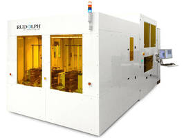
Flanders, New Jersey – Rudolph Technologies, Inc. (NYSE: RTEC) announced today that a leading outsourced assembly and test facility (OSAT) has placed an order for the JetStep® Lithography System for the semiconductor advanced packaging industry’s first panel manufacturing line. The JetStep S Series Lithography System was selected after a thorough evaluation of competitive offerings, and will be used for next-generation fan-out processing on rectangular panels. The system is scheduled to ship in mid-2016.
Mike Plisinski, Rudolph’s chief executive officer, stated, “We view the move from reconstituted wafers to chips-on-panels as a logical and necessary transition in the advanced packaging industry as product volumes increase. We are pleased that our lithography and panel solutions are able to play an integral role in this transition and look forward to partnering with these early leaders.”
According to Yole Dèveloppement’s November 2015 report, Status of Panel-Level Packaging Manufacturing1, the demand for lower cost with higher performance has driven the semiconductor industry to develop innovative solutions. One new approach to reducing overall cost is to switch from (round) wafers to a larger-size panel format. Yole describes the cost advantages and economy of scale benefits as key enablers propelling the growth of fan-out, interposers and embedded die panel packages.
“Building on more than 25 years of flat panel lithography experience, we are confident the JetStep Lithography System is a premier solution for advanced packaging panel manufacturing,” said Rich Rogoff, vice president and general manager of Rudolph’s Lithography Systems Group. “Fully capable of handling rectangular glass or organic substrates up to approximately 700mm, the JetStep System is equipped with unique features to address the challenges of lithography on panels. On-the-fly autofocus and magnification compensation enable high yields, addressing a critical challenge of fan-out to be cost effective.”
Plisinski concluded, “We have an established market presence in both fan-out wafer level packaging and radio frequency (RF) devices, which we believe will be transitioning to glass panel interposers. Our early success in advanced packaging allows us to bring a wealth of experience and knowledge to this emerging industry shift from wafers to panels. As we have partnered with our wafer customers, Rudolph will partner with panel customers, leveraging our broad range of products and resulting application expertise to not only provide lithography, but a comprehensive solution that will significantly contribute to enabling advanced packaging on panels.”
For more information about Rudolph’s JetStep Lithography systems, please visit www.rudolphtech.com.
1Yole Dèveloppement’s November 2015 report can be found at: http://bit.ly/1OrMoV4.
About Rudolph Technologies
Rudolph Technologies, Inc. is a leader in the design, development, manufacture and support of defect inspection, lithography, process control metrology, and process control software used by semiconductor and advanced packaging device manufacturers worldwide. Rudolph delivers comprehensive solutions throughout the fab with its families of proprietary products that provide critical yield-enhancing information, enabling microelectronic device manufacturers to drive down costs and time to market of their devices. Headquartered in Flanders, New Jersey, Rudolph supports its customers with a worldwide sales and service organization. Additional information can be found on the Company’s website at www.rudolphtech.com.
Rudolph Contacts:
Guerrant Associates
Laura Guerrant-Oiye
Principal
808.882.1467
lguerrant@guerrantir.com