Power SMT Packages feature fully hermetic design.
Press Release Summary:
Suited for applications in aerospace, military, and high-end industrial markets, DC and RF Hermetic SMT Packages permit power dissipation levels of 100 W and current capacity up to 75 A. Circuit designers can select multi-chip modules, BGA construction, SMT leadless and leaded I/O connections, and high-voltage insulation. Based on Plated Copper on Thick Film technology, ceramic SMT packages offer alternative to co-fired ceramic packages as well as metal-based, glass-to-metal hermetic enclosures.
Original Press Release:
Remtec Has Developed a Custom Line of Power Hermetic SMT Packages for Military, Aerospace, and High End Industrial Applications
Norwood, MA October 19, 2009. Remtec Inc., the leading manufacturer of metallized ceramic substrates and packages with Plated Copper on Thick Film (PCTF) technology has developed custom built power DC and RF hermetic SMT packages for high reliability applications in aerospace, military, and high end industrial markets. The flexibility of PCTF design and manufacturing allows easy integration of customer-specific packages into new designs and existing systems.
This advanced technology permits circuit designers to achieve high power dissipation levels (100 W), high current capacity (75 AMP), and high integration levels in light weight, compact, low profile packages which are fully hermetic (10-8) per Military Standard 883C. Since each package is designed for a specific application, circuit designers can select those package features which are best suited for their requirements. Amongst those are multi-chip modules (MCM), ball grid array (BGA) construction, SMT leadless and leaded I/O connections and high voltage insulation. Often times, PCTF ceramic SMT packages serve as an viable alternative to co-fired ceramic packages as well as metal-based glass-to-metal hermetic enclosures.
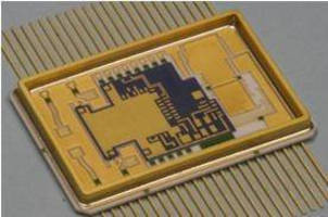
High reliability military applications often require fully-hermetic ceramic packages with built-in multi-layer circuitry, low dc resistance copper tracks, low thermal resistance (much below 1oC/W), integrated passives and thermal hermetic vias. To meet these requirements, Remtec uses advanced PCTF technology to design and fabricate a light weight, low profile package shown here. Remtec's hermetic integral substrate package (ISP) is thermally efficient and provides a high level of integration in a compact low profile size of 1.330 x .930 x.100".
In some aerospace applications, designers utilize the high current carrying capacity of PCTF plated copper tracks and hermetic vias with low DC resistance (.5 mW and less). These design characteristics allow currents in excess of 15-25 AMP in the tracks as well as directly from a flip chip to I/O connections. This unique construction results in an SMD.5 fully compatible packaging product in a standard size of .400x.296x.112".
The high reliability requirements of industrial applications such as high speed optical networks frequently necessitate hermetic leadless packages which must dissipate more than 5 W power and operate at 10 GHz. To meet these specifications, Remtec fabricated a 16 mm package with a high integration level containing a multi-chip module with integrated resistors, transmission lines and low inductance leadless SMT connections in a package .630x.630x.110".
Remtec, a RoHS compliant and ISO 9001:2000 registered company, provides custom and semi-custom packaging solutions for dc power electronics, microwave and RF components and modules, and optoelectronics.