Plasma Focused Ion Beam cuts analysis from days to hours.
Press Release Summary:
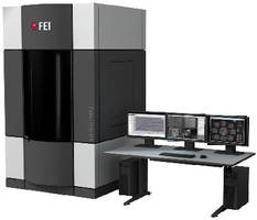
Built on DualBeam™ Plasma FIB platform with integrated SEM and nanoprobing capabilities, Helios PFIB EFI delivers site-specific sample preparation with in-situ SEM end-pointing and low-beam energy SEM-based transistor characterization. It includes electron-beam absorbed current for interconnect-level electrical fault isolation and electron-beam induced current analysis for diffusion characterization. By using FEI’s Dx delayering solution, system boosts deprocessing yields for 10 nm devices.
Original Press Release:
FEI Launches New DualBeam Plasma Focused Ion Beam for Electrical Fault Isolation and Failure Analysis
New Helios PFIB EFI is a fully-integrated deprocessing and fault isolation solution that reduces analysis time from days to just hours.
Hillsboro, Ore./—FEI (NASDAQ: FEIC) today launched a new DualBeam™ plasma focused ion beam (PFIB) for sample preparation, electrical fault isolation (EFI) and electrical failure analysis (EFA) on sub-20nm semiconductor devices. The Helios PFIB EFI is the only fully-integrated solution that improves time-to-results from days to just a few hours.
“Semiconductor process development and yield enhancement engineers no longer need to suffer delays due to a multi-tool, multi-operator approach to electrical fault isolation and failure analysis,” states Rob Krueger, vice president and general manager of FEI’s semiconductor business. “The new Helios PFIB EFI is a fully-integrated, easy-to-use solution that cuts down the number of steps and sample transfers during the process. Eliminating these bottlenecks helps to reduce the process debug and device analysis cycle time by 50-80 percent and improve yields to near 100 percent, enabling chip makers to achieve significantly faster time-to-volume manufacturing.”
The Helios PFIB EFI is built upon the world’s most advanced DualBeam Plasma FIB platform with fully-integrated SEM and nanoprobing capabilities, delivering site-specific sample preparation with in-situ SEM end-pointing and low-beam energy SEM-based transistor characterization. It includes electron-beam absorbed current (EBAC) for interconnect-level electrical fault isolation and electron-beam induced current (EBIC) analysis for diffusion characterization. The system boosts deprocessing yields for 10nm devices by using FEI’s unique Dx delayering solution.
“Our proprietary Dx beam chemistry delivers high-yield, high-throughput sample prep at the sub-16nm and 14nm nodes, while low beam-energy SEM permits accurate in situ end-pointing, high-resolution imaging and precise electrical probe positioning,” continues Krueger. “Using the Helios PFIB EFI, our customers have successfully probed devices down to contact level for complete electrical analysis without degrading the transistor’s electrical properties.”
For more information, please visit http://www.fei.com/helios-pfib-efi-for-electronics/ .
About FEI
FEI Company (Nasdaq: FEIC) designs, manufactures and supports a broad range of high-performance microscopy workflow solutions that provide images and answers at the micro-, nano- and picometer scales. Its innovation and leadership enable customers in industry and science to increase productivity and make breakthrough discoveries. Headquartered in Hillsboro, Ore., USA, FEI has over 2,600 employees and sales and service operations in more than 50 countries around the world. More information can be found at: www.fei.com.