Photolithography Service can produce patterned optical filters.
Press Release Summary:
Photolithography services support patterning 200 mm dia wafers. By fusing together information from different wavelength bands, patterning provides enhanced view or enhanced detection in multi-spectral imaging tasks. Populated wafers containing active devices can also be patterned. Applications include satellite imaging, UAV overhead reconnaissance, machine vision, food and industrial inspection, automotive, biomedical sensing, color filter arrays for CCD/CMOS cameras, and reticles.
Original Press Release:
Deposition Sciences Increases Photolithography Patterning Capacity
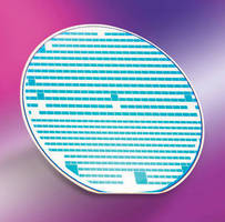
• New 200 mm diameter wafer enhances photolithography capability
Santa Rosa, CA – Deposition Sciences, Inc. (DSI®), manufacturer of highly durable thin film optical coatings, introduces an enhanced capability to manufacture patterned optical filters. DSI has increased its capacity and resolution with the introduction of a new photolithography production line capable of patterning 200 mm diameter wafers.
Director of marketing and sales, Michael Newell, notes, “We are very excited to announce this enhanced capability. This new manufacturing line brings us better resolution, increased capacity, an ability to yield and coat more parts per wafer, and ultimately better pricing for our customers. And we are keeping pace with the semi-conductor industry. Customers are looking to integrate their electronics with the optical filters. DSI can pattern populated wafers containing active devices, and semi-conductor fab houses are doing more and more at the 200 mm wafer scale.”
The new patterning capability provides an enhanced view or enhanced detection in multi-spectral imaging tasks by fusing together information from different wavelength bands. Other applications include satellite imaging, UAV overhead reconnaissance, machine vision, food and industrial inspection, automotive, biomedical sensing, color filter arrays for CCD and CMOS cameras, reticles, and more. For more information on DSI’s 200 mm diameter photolithography patterning capability, please visit: www.depsci.com.
Deposition Sciences, Inc. (DSI) – Santa Rosa, CA – www.depsci.com - For over 25 years, Deposition Sciences has produced the most durable optical thin film filter coatings in the industry. DSI’s coating capability ranges from the ultraviolet (UV), through the visible and includes near-infrared (NIR), midwave-infrared (MWIR) and out to the longwave-infrared (LWIR). At the heart of these capabilities is DSI’s patented MicroDyn® reactive sputtering technology enabling superior multilayer thin film coatings for optics and other thin film technologies.
Deposition Sciences, Inc. (DSI)
3300 Coffey Lane
Santa Rosa, CAÂ 95403
Contact: Tatiana Atkinson
Inside Sales Manager
Phone: 707-573-6785
Fax: 707-573-6748
Email: Solutions@depsci.com
Web Site:Â www.depsci.com
Marlene D. Moore
Advertising • Marketing • Public Relations – for Advanced Technologies
818-708-1704 / Fax: 818-344-7179
Cell: 818-512-6090
marlene@smithmillermoore.com