OKI Establishes World's First Mass-production Technology for 0.35 mm pitch 1,000 pin LSI 30-layer Printed Circuit Boards
Share:
Breakthrough made possible using OKI's FiTT method based on high-precision lamination and high-precision drilling
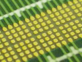
Enlarged view of 0.35 mm pitch
socket connections on a 30-layer
3.5 mm thick socket board
TOKYOÂ – Oki Printed Circuits Co., Ltd. (hereinafter "OKI Printed Circuits"), an OKI Group company responsible for printed circuit board business, recently established a mass-production technology for printed circuit boards having a maximum board thickness of 3.5 mm (30 layers) to support next-generation 1,000-pin LSIs with a pin pitch of 0.35 mm, which are expected to see future use in various smart devices such as smartphones. The mass production commenced in December 2014 on printed circuit boards for socket boards used in LSI function testing devices (LSI testers).
As mobile devices such as smartphones grow smaller and more powerful, the LSIs inside them have also grown ever smaller, with pin pitch falling from 0.50 mm or 0.40 mm to 0.35 mm. Development has also begun of highly functional LSIs having more than 1,000 pins to achieve the performance needed to transmit large volumes of data at high speeds. The printed circuit boards needed to test the functionality of such next-generation LSIs must support reduced pitch, better handle signals associated with the increased number of pins, and ensure a stable power supply and grounding for the increased number of signals. These requirements necessitate more layers, something not possible with existing manufacturing technologies. This presented a major obstacle to the mass production of next-generation LSIs.
In response, OKI Printed Circuits developed its new FiTT (Fine pitch Through via Technology) method, which is capable of forming through vias of ultrafine diameters (finished diameter 0.10 mm) with a pitch of 0.35 mm in substrates with a maximum board thickness of 3.5 mm (30 layers), a feat not possible with existing build-up method (Figure 1) or through via method. What made possible the world's first mass-production technology for producing 0.35 mm pitch 1,000+ pin printed circuit boards of large number of layers are high-precision laminating technologies, which minimize layer-to-layer registration offsets to within 40 µm, and high-precision drilling technologies, which use systems for adjusting via hole positions down to the micron level and optimize drill shape and drilling process steps. This technology is capable of ensuring a stable power supply and grounding connections, even with large number of layers for through via configurations, thereby achieving the high signal quality required by the circuit boards used in LSI function testing devices. Moreover, the simplicity of the process allows production at low cost and short lead times.
OKI Printed Circuits plans to take an active approach to expanding its printed circuit board business to handle narrow-pitch multi-pin LSIs beyond the reach of previous methods. The company will target the market for LSI tester socket boards. OKI Printed Circuits is also working to develop next-generation printed circuit boards (with pitches of 0.30 mm or less) as part of efforts to develop products to match customer requirements.
OKI Printed Circuits will exhibit this technology at NEPCON JAPAN 2015 Printed Circuit Boards EXPO, to be held at Tokyo Big Sight from January 14 to 16, 2015.
About OKI Electric Industry (OKI)
Founded in 1881, OKI Electric Industry is Japan's leading telecommunications manufacturer in the Info-telecom field. Headquartered in Tokyo, Japan, OKI provides top-quality products, technologies, and solutions to customers through its info-telecom systems and printer operations. Its various business divisions function synergistically to bring to market exciting new products and technologies that meet a wide range of customer needs in various sectors. Visit OKI's global website at http://www.oki.com/.
The names of the companies and products mentioned in this document are the trademarks or registered trademarks of the respective companies and organizations.
Press Contact:
Public Relations Division
Phone: +81-3-3501-3835