New Semiconductor Lithography System with Optional Through-Silicon Alignment System
Press Release Summary:
- FPA-3030i5a is designed to process small substrates between 50 and 200 mm in diameter
- Features chamber temperature control system and employs a high-speed wafer feeding system
- Supports silicon wafers as well as common compound semiconductor materials such as SiC and GaN
Original Press Release:
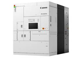
Canon to Commence Sales of The FPA-3030i5a Semiconductor Lithography System in March 2021, Supporting Reduced Cost-of-Ownership Manufacturing for Small Substrates
MELVILLE, N.Y., Dec. 1, 2020 /PRNewswire/ -- Canon U.S.A., Inc. today announced that its parent company, Canon Inc., will commence sales of the FPA-3030i5a in March 2021. The FPA-3030i5a is the newest entry in the Company's lineup of i-line1 semiconductor lithography systems supporting manufacturing of devices including compound semiconductors. The FPA-3030i5a is also designed to help reduce cost of ownership (CoO), an indicator of the total cost required for semiconductor manufacturing.
The FPA-3030i5a semiconductor lithography system, or stepper, is designed to process small substrates between 50 mm (2 inches) and 200 mm (8 inches) in diameter. FPA-3030i5a steppers support not only silicon wafers, but also common compound semiconductor materials such as SiC (silicon carbide) and GaN (gallium nitride), which helps enable the manufacturing of various semiconductor devices that are expected to see increased demand in the future, such as high-power devices for automobile electrification and high-bandwidth video processing and communication devices for 5G communication.
FPA-3030i5a stepper hardware and software have been upgraded from its predecessor, the FPA-3030i5+ stepper (released in June 2012), to help reduce CoO*. The FPA-3030i5a inherits the imaging performance of the FPA-3030i5, achieving exposure resolution of 0.35 micrometer2 line width patterns while providing robust alignment options and increased productivity. The FPA-3030i5a employs a high-speed wafer feeding system that can be configured to handle a variety of wafer materials and sizes including compound semiconductors with a diameter from 50 mm to 200 mm.
The FPA-3030i5a uses a new off-axis alignment scope to illuminate and measure wafer alignment marks. By not observing the marks through the projection lens, the FPA-3030i5a alignment system can employ a wide range of illumination wavelengths to help optimize alignment conditions. FPA-3030i5a steppers equipped with the optional Through-Silicon Alignment (TSA) system can also utilize infrared light to view through substrates to enable backside alignment processes. The new alignment system in the FPA-3030i5a also shortens alignment mark measurement time*.
The reduced alignment time, high-speed feeder system and upgraded software allow the FPA-3030i5a to achieve 123 wafers per hour (wph) output for 200 mm (8 inch) wafers, which is approximately a 17 percent productivity improvement compared to its predecessor*. FPA-3030i5a steppers also feature a new chamber temperature control system that maintains the lithography system in a clean environment and constant temperature level. The new design helps reduce FPA-3030i5a stepper power consumption by approximately 20 percent compared to the predecessor model and through such improvements, the system helps reduce CoO*.
Through the introduction of the FPA-3030i5a and implementation of advanced functions, system owners are able to manufacture specialty power and communication devices using a wide range of wafer materials including silicon and compound semiconductors such as SiC and GaN ranging in size from 50 mm to 200 mm.
FPA-3030i5a semiconductor lithography systems are expected to go on sale in early March 2021.
About Canon U.S.A., Inc.
Canon U.S.A., Inc. is a leading provider of consumer, business-to-business, and industrial digital imaging solutions to the United States and to Latin America and the Caribbean markets. With approximately $33 billion in global revenue, its parent company, Canon Inc. (NYSE:CAJ), ranks third overall in U.S. patents granted in 2019† and was named one of Fortune Magazine's World's Most Admired Companies in 2020. Canon U.S.A. is dedicated to its Kyosei philosophy of social and environmental responsibility. To keep apprised of the latest news from Canon U.S.A., sign up for the Company's RSS news feed by visiting www.usa.canon.com/rss and follow us on Twitter @CanonUSA.
A semiconductor lithography system that utilizes a 365 nm wavelength mercury lamp as the light source. 1 nm (nanometer) is 1 billionth of a meter.
1 micrometer is 1 million times 1 meter (= 1000/1mm).
According to Canon research and public third party data, as well as industry information as of June 22nd, 2020.
Based on weekly patent counts issued by United States Patent and Trademark Office.
Availability and specifications are subject to change without notice.
Source Canon U.S.A., Inc.
Contact:
Eloise Pisano, Canon U.S.A., Inc., 631.330.5195, episano@cusa.canon.com