New Model 54851 Includes Multi-board Clock, Sync Engine and Large DDR4 memory
Press Release Summary:
- Features 2 500 MHz 12-bit A/Ds with 2 programmable multiband digital downconverters and 1 digital upconverter with 2 800 MHz 16-bit D/As
- Includes high-bandwidth connections to Kintex UltraScale FPGA for custom digital I/O
- Designed for air-cooled, conduction-cooled and rugged operating environments
Original Press Release:
Pentek’s New 3U VPX Board Optimizes High-speed Optical and RF I/O Connectivity
- OpenVPX Compliant Optical and RF I/O to VPX Backplane
- Jade Architecture with Xilinx Kintex Ultrascale FPGA offers price, power and processing performance advantages
- Navigator Design Suite expedites development and custom IP integration
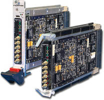
Upper Saddle River, NJ ─ April 29, 2019 ─ Pentek, Inc., today introduced the newest member of the Jade™ family of high-performance 3U VPX boards. The Model 54851 is based on the Xilinx Kintex Ultrascale FPGA and features two 500 MHz 12-bit A/Ds with two programmable multiband digital downconverters (DDCs) and one digital upconverter (DUC) with two 800 MHz 16-bit D/As. The 54851 is the first board utilizing this new 3U VPX architecture with advanced wideband I/O options.
“Recent enhancements to OpenVPX have greatly improved I/O capabilities,” said Robert Sgandurra, director of Product Management. “These enhancements play well into Pentek’s modular approach to product design by offering optical and RF options for high-performance I/O that perfectly match our product capabilities.”
The Model 54851 takes advantage of these VPX I/O options for RF and optical interconnects through the VPX backplane:
- Option -110: Optical connections based on VITA 66.5 (draft), containing blind-mate MT optical connectors with fixed contacts on the plug-in module and floating displacement on the backplane.
- Option -111: RF connections based on ANSI/VITA 67.2, containing multi-position blind-mate analog connectors with SMPM contacts.
- Option -112: RF connections based on ANSI/VITA 67.3 type C, containing multi-position blind mate analog connectors with SMPM contacts, spring-loaded on the backplane allowing more movement and larger diameter cables for better performance.
Future options for higher density optical and RF connectors are planned as the supporting standards become available. Organizations such as The Open Group Sensor Open Systems Architecture (SOSA™) Consortium are specifying additional types and apertures for VITA 67.3.
The Model 54851 can be populated with a range of Kintex UltraScale FPGAs to match specific requirements of the processing task, spanning from the entry-level KU035 (with 1,700 DSP slices) to the high-performance KU115 (with 5,520 DSP slices). The KU115 is ideal for demanding modulation/demodulation, encoding/decoding, encryption/decryption, and channelization of the signals between transmission and reception. For applications not requiring large DSP resources or logic, a lower-cost FPGA can be installed.
The Model 54851 also includes a complete multi-board clock and sync engine and a large DDR4 memory. In addition to supporting PCI Express Gen. 3 as a native interface, the Model 54851 includes optional high-bandwidth connections to the Kintex UltraScale FPGA for custom digital I/O.
With the Xilinx Kintex Ultrascale FPGA, data converters and optical or RF I/O, the Model 54851 becomes an excellent high performance interface to HF or IF ports of a communications or radar system.
The Jade Architecture
The Pentek Jade architecture is based on the Xilinx Kintex UltraScale FPGA, which raises the digital signal processing (DSP) performance by over 50% with equally impressive reductions in cost, power dissipation and weight. Its PCI Gen.3 interface allows access to control and status registers for controlling algorithms, state machines and data flow across the LVDS I/O front panel and carrier board interfaces. A 5 GB bank of DDR4 SDRAM is available for additional functions. The factory-installed DMA controller can sustain 6.4 GB/s data transfers across PCIe.
Navigator Design Suite for Streamlined IP Development
Pentek’s Navigator™ Design Suite was designed from the ground up to work with Pentek’s Jade architecture and Xilinx’s Vivado Design Suite® providing an unparalleled plug-and-play solution to the complex task of IP and control software creation and compatibility. Graphical design entry for Xilinx and Pentek AXI4-compliant IP modules using the Xilinx IP Integrator greatly speeds development tasks. The Navigator Design Suite consists of two components: Navigator FDK (FPGA Design Kit) for integrating custom IP into Pentek sourced designs and Navigator BSP (Board Support Package) for creating host applications. Users can work efficiently at the API level for software development and with an intuitive graphical interface for IP design. The Navigator BSP is available for Windows and Linux operating systems.
Pricing and Availability
Designed for air-cooled, conduction-cooled and rugged operating environments, the Model 54851 XMC module with 5 GB of DDR4 SDRAM starts at $12,595 USD. Delivery is 10 to 12 weeks ARO. The Navigator Design Suite consists of two packages. The Navigator BSP is $2,500 USD and the Navigator FDK is $3,500 USD.
About Pentek
Pentek, an ISO 9001:2015 certified company, designs and manufactures innovative commercial and rugged DSP boards and real-time system recorders for commercial, government and military systems including radar, communications, SIGINT, defense, medical and industrial control applications. Pentek offers powerful VPX, FMC, FMC+, AMC, XMC, cPCI and PCIe board solutions featuring high-performance Xilinx FPGAs. Pentek equips all boards and recorder products with high-performance I/O including gigabit serial interfaces, powerful software development tools and offers strong DSP software support.
Media Contact:
Barbara Stewart
Patterson & Associates
480-488-6909