New Fujitsu FRAM Devices Combine the Benefits of Fast-Writing SRAMs with Flash in a Single IC for Industrial, Factory, and Low-Power Applications
Share:
o Latest MB85RSxxx SPI Series, MB85RCxxx I2C Series and FRAM-based RFIDs Designed and Manufactured by Fujitsu Will Meet the Rapidly Increasing Global Demand for FRAM Solutions
SUNNYVALE, Calif. - Fujitsu Semiconductor America, Inc. (FSA) today introduced a new series of advanced Ferroelectric Random Access Memory (FRAM) products designed and manufactured by Fujitsu to meet the rapidly increasing demand for FRAM in industrial systems, factory automation, metering, and many other low-power applications that require high-performance, non-volatile memory.
The new MB85RSxxx SPI FRAM family includes three different devices: the 256-Kbit MB85RS256A, the 128-Kbit MB85RS128A and the 64-Kbit MB85RS64A. All three operate at voltage ranges between 3.0V and 3.6V and provide an industry-leading 10 billion write/read cycles, as well as data retention of 10 years at 55 degrees C.
The new series is based on Fujitsu's latest 0.18um (micron) FRAM technology and features a maximum operating frequency of 25MHz, a significant improvement over the company's previous FRAM devices. Since voltage boosters are unnecessary for the writing process, the new FRAMs are well-suited for low-power applications. All the MB85RSxxx series devices are offered in 8-pin, plastic SOP packages with standard memory pin assignment, which are fully compatible with E2PROM devices.
In addition to the SPI FRAM family, Fujitsu also has developed standalone FRAM devices featuring the I2C (MB85RCxxx series) and parallel interfaces (MB85Rxxx series). These standalone devices are available in density levels ranging from 16Kbit to 1Mbit and with a product roadmap that includes higher densities to meet future market demands.
High-Density RFID Chip Also Sampling
Fujitsu also is sampling its high-performance, high-density RFID chips. These high-frequency FRAM-based RFID products, which comply with the ISO/IEC 15693 and ISO/IEC18000-3 standards, are available in 256-bytes and 2Kbytes memory variations. In addition, Fujitsu is sampling RFIDs that comply with EPC Global Gen 2, and which provide 4Kbytes of FRAM and an alternate SPI interface.
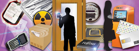
Fujitsu's near-term roadmap includes the industry's largest 64Kbytes EPC Global Gen 2 RFID chip. This family of high-density, FRAM-based RFID products enables robust tracking applications. The chips offer a traceable audit trail at the item level that includes not just a basic identification code, but also detailed historical, tracking or other records that trace an object through the supply chain and throughout its lifecycle. Since FRAM has a high tolerance against radiation, these RFID chips are suitable for various medical and pharmaceutical applications.
Assured Reliable, Stable FRAM Supply
The industry's largest FRAM supplier, Fujitsu was the first company to embed FRAM into CMOS logic in 1998 and to release the industry's first mass production quantities in 1999. Fujitsu couples its highly reliable and proven manufacturing capabilities with optimized FRAM design to produce the industry's highest quality FRAM products.
Tong Swan Pang, senior manager of marketing at Fujitsu Semiconductor America, cited the benefits to global markets of the company's ability to control design, manufacturing process technology and production schedules. "Fujitsu recently completed the migration of FRAM products from the company's older line in the Iwate fabrication facility to a newer line in Mie, Japan, which has been manufacturing ICs using the highly-efficient 0.18 micron technology for several years," he said "Because Fujitsu owns its fabrication facilities, the company can ensure a more reliable and stable supply to meet the steadily increasing market demand for FRAM products. This is a key advantage that Fujitsu offers its customers compared to fabless suppliers that out-source their production and thus might be subject to supply interruptions."
A non-volatile memory with data retention of at least 10 years, FRAM can ideally replace all battery back-up solutions and enable environmentally friendly products. FRAM standalone memory devices are widely used in metering and factory automation applications as well as in various industrial segments where data logging, high-speed write access and high endurance is essential. The ferroelectric material in FRAM is highly resistant to magnetic fields and radiation, making it also well-suited for applications in the medical, aerospace and food industries.
For more information about Fujitsu FRAM technology and products, visit http://us.fujitsu.com/semi/fram.
About Fujitsu Semiconductor America, Inc.
Fujitsu Semiconductor America, Inc. (FSA) is a leading designer and developer of innovative semiconductor products and solutions for new generations of consumer, communications, automotive and industrial products. FSA provides a comprehensive portfolio of high-quality, reliable semiconductor products and services throughout North and South America. Founded in 1979 and headquartered in Sunnyvale, California, Fujitsu Semiconductor America (formerly Fujitsu Microelectronics America) is a wholly owned subsidiary of Fujitsu Semiconductor Limited (FSL), Japan.
For product information, visit the company's website at us.fujitsu.com/semi, e-mail FSA_inquiry@us.fujitsu.com or call 1-800-866-8608. For company news and updates, connect with FSA on Twitter at http://twitter.com/FujitsuSemiUS.
Reference Material
FRAM Product Web Page: http://us.fujitsu.com/semi/fram
FRAM Product Image (version 1 - banner): http://www.fujitsu.com/downloads/MICRO/fsa/pr/images/2011/FRAM0511.jpg
FRAM Product Image (version 2 - square) http://www.fujitsu.com/downloads/MICRO/fsa/pr/images/2011/FRAM0711.jpg
SOURCE Fujitsu Semiconductor America, Inc.
CONTACT: Steven Wolpern of Fujitsu Semiconductor America, Inc., +1-408-737-5625, FSA_PR@us.fujitsu.com; or Dick Davies of IPRA, 1-415-652-7515, ipra@mindspring.com
Web Site: www.fma.fujitsu.com