Mask Alignment System manufactures high-brightness LEDs.
Press Release Summary:
Equipped with high-intensity UV light source and optional filter fan unit, EVG620HBL Gen II provides wafer throughput up to 165 6-in. wafers/hr. Robotic handling layout with wafer mapping capability supports demand for wafer traceability, while microscope supports automated mask pattern search, minimizing mask setup and change time. With recipe-controlled microscopes, illumination spectrum can be varied to ensure best pattern contrast with various wafer and layer materials.
Original Press Release:
EV Group Launches Second-Generation EVG620HBL Mask Alignment System for LED Manufacturing
Updated HB-LED Manufacturing Tool Commands Unprecedented Cost of Ownership Advantages
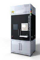
SANTA CLARA, Calif., -- STRATEGIES IN LIGHT -- EV Group (EVG), a leading supplier of wafer-bonding and lithography equipment for the advanced semiconductor and packaging, compound semiconductors, MEMS, silicon-on-insulator (SOI) and emerging nanotechnology markets, today announced the EVG620HBL Gen II--the second generation fully automated mask alignment system for volume manufacturing of high-brightness light-emitting diodes (HB-LEDs). Introduced one year after the launch of the first-generation EVG620HBL, the Gen II delivers a tool platform tailored to address HB-LED customer-specific needs and the ongoing demand of total cost-of-ownership reduction. The EVG620HBL Gen II also optimizes tool footprint in the fab--delivering 55 percent higher wafer output for every square meter of cleanroom space compared to competitive offerings.
Dr. Thomas Uhrmann, business development manager for EV Group, noted, "The HB-LED market is dynamic and fast changing, and our customers constantly need innovative solutions to ensure their output and capital investments are being maximized. The EVG620HBL Gen II is a great example of how EVG quickly responds to its customers' needs by leveraging its expertise in HB-LED manufacturing to deliver an effective solution. Having already built a proven platform that is now a de-facto industry standard with our first-generation mask alignment tool, we expect the EVG620HBL Gen II will further widen the economical gap over competitive offerings." Today, EVG's bonders and mask aligners are being deployed by four of the top five major HB-LED manufacturers.
Escalating demands for cost reductions and yield enhancements require that equipment providers rethink what they bring to the table in terms of total cost of ownership. This is particularly true with mask alignment for lithography where maximizing yield is critical to fulfilling the long-term growth potential of LED technology. The EVG620HBL Gen II is outfitted with a host of new features aimed at satisfying high-volume manufacturing (HVM) customers' specific demands:
-- Enhanced microscope supporting automated mask pattern search, which further reduces mask setup and change time--both of which are critical to enabling continuous device production in HVM environments;
-- Updated robotic handling layout with wafer mapping capability, which supports the demand for wafer traceability;
-- Improved alignment capability (line alignment), which leverages the grids that mark single LEDs for orientation instead of requiring alignment marks that take up valuable space on the wafer;
-- Reduced system footprint, which optimizes total cost of ownership for operation and increases the wafer per footprint index.
Together, these key enhancements to the EVG620HBL Gen II enable a 20-percent reduction in cost-per-processed wafer compared to competitive offerings.
Built on EVG's field-proven mask aligner platform, the EVG620HBL series features a high-intensity ultraviolet (UV) light source and an optional filter fan unit to maximize yield and enable the industry's highest wafer throughput of up to 165 six-inch wafers per hour (up to 220 wafers per hour in first print mode). Another key feature of the EVG620HBL is the availability of special recipe-controlled microscopes whose illumination spectrum can be varied and optimized to ensure the best pattern contrast with various wafer and layer materials, including such advanced substrate materials as sapphire, silicon carbide (SiC), aluminum nitride (AlN), metal and ceramic. The EVG620HBL series processes 2- to 6-inch wafers.
The EVG620HBL Gen II is available for purchase immediately. For more information about this tool, please visit www.evgroup.com or visit the company at the Strategies in Light Conference in Santa Clara, Calif. from February 7-9, 2012. EVG's Dr. Thomas Uhrmann will present on "High Throughput Lithography and Metal Wafer Bonding: Two Enabling Technologies for Future High-Brightness LEDs" at the conference on Thursday, February 9 at 8:30 a.m. Pacific Time.
About EV Group
EV Group (EVG) is a world leader in wafer-processing solutions for semiconductor, MEMS and nanotechnology applications. Through close collaboration with its global customers, the company implements its flexible manufacturing model to develop reliable, high-quality, low-cost-of-ownership systems that are easily integrated into customers' fab lines. Key products include wafer bonding, lithography/nanoimprint lithography (NIL) and metrology equipment, as well as photoresist coaters, cleaners and inspection systems.
In addition to its dominant share of the market for wafer bonders, EVG holds a leading position in NIL and lithography for advanced packaging and MEMS. Along these lines, the company co-founded the EMC-3D consortium in 2006 to create and help drive implementation of a cost-effective through-silicon via (TSV) process for major ICs and MEMS/sensors. Other target semiconductor-related markets include silicon-on-insulator (SOI), compound semiconductor and silicon-based power-device solutions.
Founded in 1980, EVG is headquartered in St. Florian, Austria, and operates via a global customer support network, with subsidiaries in Tempe, Ariz.; Albany, N.Y.; Yokohama and Fukuoka, Japan; Seoul, Korea and Chung-Li, Taiwan. The company's unique Triple i-approach (invent - innovate - implement) is supported by a vertical integration, allowing EVG to respond quickly to new technology developments, apply the technology to manufacturing challenges and expedite device manufacturing in high volume. More information is available at www.EVGroup.com.
CONTACT: Clemens Schutte, Director, Marketing and Communications of EV Group, +43 7712 5311 0, Marketing@EVGroup.com
Web Site: www.evgroup.com