Logic Module supports SoC/ASIC prototyping.
Press Release Summary:
Using 4 Xilinx Virtex®-7 2000T All Programmable 3D ICs, Quad V7 TAI Logic Module allows designers to deploy multiple SoC/ASIC prototypes for hardware verification and early software development. Module supports 80+ pairs length-matched LVDS bus between any 2 FPGAs optimized for LVDS pin-multiplexing and 10,000+ design interconnections between any 2 FPGAs with LVDS bus running at 800 MHz+. With dedicated LVDS Pin-Multiplexing reference clocks and reset circuits, almost any design can be partitioned.
Original Press Release:
New Quad Virtex-7 2000T 3D IC Rapid ASIC Prototyping Platform from S2C Optimized for Design Partitioning
S2C Virtex-7 Series TAI Logic Module is compatible with previous generations and provides large library of daughter cards
San Jose, CA – S2C Inc. today announced the addition of the newest prototyping platform, Quad V7, to its V7 TAI Logic Module series, a new generation of SoC/ASIC prototyping hardware based on Xilinx’s Virtex®-7 2000T All Programmable 3D ICs.
S2C’s V7 TAI Logic Module series use up to 9 Virtex-7 2000T devices on a single board to make SoC/ASIC prototyping a productive experience for designs of any size from 20 million up to 180 million ASIC gates. S2C has integrated Xilinx’s Vivado™ Design Suite in its prototype creation software flow and ChipScope™ Pro tools in its debug software for accelerated design productivity. In addition, the Quad V7 TAI Logic Module hardware is designed to run high-frequency pin-multiplexing through LVDS interconnection bus to fit designs when partitioned to multiple FPGAs.
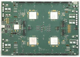
S2C Quad 7V2000T TAI Logic Module
“Xilinx’s Virtex®-7 2000T All Programmable 3D ICs with their Stacked Silicon Interconnect (SSI) technology are changing the landscape of SoC/ASIC prototyping by enabling advanced system integration capabilities. SSI technology allows multiple die to be combined in a single package to deliver almost 3 times more logic, memory, serial transceivers, and processing elements than previously available FPGAs,” noted Mon-Ren Chene, Chairman and CTO of S2C. “Rapid FPGA-based prototyping has become a critical step for a successful SoC product launch but was not a viable option when design sizes were extremely large. With four Virtex®-7 2000T All Programmable 3D ICs on a single SoC/ASIC prototyping platform, designers can now fit a fairly large design such as an SoC with multi ARM-A15 Cores and multi GPU cores. Traditionally, complex SoC verification has been performed by using expensive emulators that run only at a small fraction of real clock speed, making software development painful.
“S2C’s Quad V7 TAI Logic Modules now allows designers to deploy multiple SoC/ASIC prototypes for both hardware verification and early software development, so the overall SoC design cycle can be greatly reduced. On the technical aspect, we have designed the interconnections between the 4 All Programmable devices to run large number of LVDS pairs synchronously at over 800MHz. With dedicated LVDS Pin-Multiplexing reference clocks and reset circuits, almost any design can be partitioned easily to our Quad V7 TAI Logic Module.”
“We are pleased to see S2C among the first few vendors in the Alliance Program ecosystem to offer an ASIC prototyping system based on the world’s largest All Programmable device," noted Dave Tokic, Sr. Director, Partner Ecosystems and Alliances at Xilinx. “S2C has a long history of providing value to the ASIC prototyping community through Xilinx-based rapid prototyping boards leveraging Virtex-6, Virtex-5, Virtex-4 and Virtex-II-Pro FPGA families.”
About LVDS Pin-Multiplexing Interconnection Support
S2C’s Quad V7 TAI Logic Module is architected to run pin-multiplexing using LVDS pairs at high-frequency. Users can use either third party partition tools or optional S2C TAI Player Pro software to map a design to the four Virtex-7 2000T devices. Â
• Supports 80+ pairs length-matched LVDS bus between any 2 FPGAs optimized for LVDS Pin-Multiplexing
• Supports 10,000+ design interconnections between any 2 FPGAs with LVDS bus running at 800MHz+
• On-board high-quality programmable LVDS Pin-Multiplexing clock source
• Dedicated LVDS Pin-Multiplexing reference clocks without consuming user resource and dedicated Reset button for initializing Pin-Multiplexing before user design starts
About S2C V7 TAI Logic Modules
The V7 TAI Logic Module series, S2C’s fifth generation products, are designed to make prototyping feasible and pleasant experience for designs of any size from 20 Million up to 180 Million ASIC gate equivalent with 1 to 9 Xilinx Virtex-7 2000T devices on a single board. Multiple V7 TAI Logic Modules can be stacked or tiled to scale up to meet higher gate capacity requirements.Â
The V7 TAI Logic Module has many significant improvements to facilitate higher system prototype performance, reliability and ease-of-use through enhanced remote resource management, power management, clock management and cooling mechanisms. The V7 TAI Logic Module now supports the following hardware control functions through both the USB and Ethernet interface from a Windows or Linux machine.
• Fast FPGA design download with multiple options – JTAG, USB, SD Card and Ethernet
• Comprehensive Self-Test for all I/O, interconnections and clocks
• Program clocks, select clock sources and adjust on-board programmable clock frequencies
• Remote hardware control via Ethernet interface – Reset, configure FPGA design and execute run-time utilities
• Monitor on-board voltage, current and temperature and automatically take corrective action upon limits violation
• Read-back hardware information - global clock frequencies, hardware type, firmware details etc.
• Adjust I/O voltages, FPGA cooling fan speed through software
• Enables re-use of daughter cards designed for previous generation prototyping systems such as Virtex-6 or Virtex-5 TAI LM systems
S2C also provides optional prototype creation and multi-FPGA debug software; DPI, SCE-MI and C-API co-modeling; and, a large library of off-the-shelf Prototype Ready IP & Accessories to speed up the creation of design prototypes using the V7 TAI Logic Modules.
The Quad TAI Logic Module starts shipping now. The Single and Dual V7 TAI Logic Modules have been shipping since June 2012. The Nine TAI Logic Module is scheduled to release in Q2 of 2013.Â
About S2C
Founded and headquartered in San Jose, California, USA. S2C has been successfully delivering rapid SoC prototyping solutions since 2003. S2C provides:
• Rapid FPGA-based SoC prototyping hardware and automation software
• Prototype Ready™ IP, Platforms, and Accessories
• System-level design verification and acceleration
S2C's value is our singular focus on SoC/ASIC development. Our highly qualified engineering team and customer-focused sales force understands our customers’ SoC development needs. S2C’s unique FPGA-based solution, using our patented TAI IP technology, enables designers to quickly assemble FPGA-based SoC prototypes on S2C FPGA boards. This gives customers an early start on software development, typically the long pole item in development schedules. Combining rapid prototyping methodologies with a comprehensive portfolio of Prototype Ready IP and advanced verification and acceleration solutions, S2C solutions greatly reduces the SoC design cycle.
In addition to the headquarters in San Jose, CA, S2C currently has 4 direct offices located in Shanghai, Beijing, Shenzhen China
and HsinChu, Taiwan. For more information, visit www.s2cinc.com.
Media Contact:
Michel Cao, S2C, China, Phone: +86 21 6887 9287, Email: michelc@s2cinc.com
Ashok Kulkarni, S2C, USA, Phone: +1 408 213 8818 x820, Email: ashokk@s2cinc.com
S2C, Prototype Ready and TAI, are trademarks of S2C, Inc. All other trade names and trademarks are the property of their respective owners.