Latest NovusEdge Inspection System Uses Multiple Cameras
Press Release Summary:
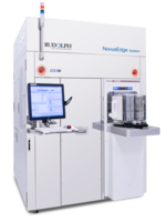
The NovusEdge™ System is designed for edge, notch and backside inspection of unpatterned wafers. The system is offered with multiple cameras, advanced technologies for delivering composite image of the entire wafer bevel. The device uses sophisticated analytical routines for identifying and classifying defects as small as the sub-micron level. It utilizes high-speed laser-scanning to detect particles, scratches, area defects and haze.
Original Press Release:
Rudolph Technologies Releases NovusEdge System for Edge, Notch and Backside Inspection of Unpatterned Wafers
New system combines high sensitivity, repeatability and throughput to deliver the industry’s best performance and cost-of-ownership for inspection of critical wafer zones
Wilmington, Mass. (November 1, 2018)—Rudolph Technologies, Inc. (NYSE: RTEC) today announced the availability of its NovusEdge™ system for edge, notch and backside inspection of unpatterned wafers. The company plans to ship multiple systems totaling more than $3M by year end to fill existing orders from two customers. The new system is the result of a multi-year collaboration with bare wafer manufacturing partners that require one inspection tool capable of detecting defects near the wafer’s edge, bevel, back-side and notch. The NovusEdge system meets the stringent new requirements for defect control at the edge and backside of wafers being manufactured for 10nm process nodes. The system provides up to 50 percent faster throughput and two orders of magnitude better edge sensitivity than incumbent technology.
“Gartner estimated the unpatterned wafer inspection market at over $400M in 2017,” Tim Kryman, senior director of product marketing explained. “The bulk of this is focused on finding front surface defects as small as 10nm. However, our development partners also required tighter defect control at the wafer bevel and backside, to ensure the stringent quality standards required for these process nodes. We estimate the NovusEdge system’s addressable market at 15 – 20 percent of the overall unpatterned market.”
The NovusEdge system uses multiple cameras and advanced imaging technologies to build a high-resolution, composite image of the entire wafer bevel then applies sophisticated analytical routines to identify and classify defects as small as the sub-micron level. On the backside it utilizes high-speed laser-scanning to detect particles, scratches, area defects and haze.
For more information about Rudolph’s inspection solutions, visit www.rudolphtech.com.
About Rudolph Technologies
Rudolph Technologies, Inc. is a leader in the design, development, manufacture and support of defect inspection, lithography, process control metrology, and rocess control software used by semiconductor and advanced packaging device manufacturers worldwide. Rudolph delivers comprehensive solutions throughout the fab with its families of proprietary products that provide critical yield-enhancing information, enabling microelectronic device manufacturers to drive down costs and time to market of their devices. Headquartered in Wilmington, Massachusetts, Rudolph supports its customers with a worldwide sales and service organization. Additional information can be found on the Company’s website at www.rudolphtech.com.
Contacts:
Investors: Trade Press:
Michael Sheaffer Sandy Fewkes
978.253.6273 408.224.4024