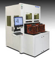
IR Metrology System measures bond parameters of 3DS-ICs.
Press Release Summary:
Utilizing confocal IR laser scanning microscope technology, 3DIR Metrology and Defect Review System measures post bond parameters of 3D stacked integrated circuits, such as overlay alignment accuracy, bonding interface thickness variations, and bonding interface quality. System measures alignment points at selected die of bonded wafers, stores images and data, and summarizes results. Correlation of overlay alignment offset data to electrical yield provides early indication of bonded wafer yield.
Original Press Release:
Olympus-ITA Introduces 3DIR Metrology and Defect Review System at SEMICON West, Booth 1524
~ IR metrology is an early indicator of electrical yield in bonded wafer pairs ~
San Jose, CA. - Olympus Integrated Technologies America, Inc. (Olympus-ITA), a leader in advanced inspection and defect review systems, introduces the latest 3DIR Metrology and Defect Review System at SEMICON West 2011, booth #1524. The system uses a confocal IR laser scanning microscopy technology for measuring post bond parameters of three dimensional stacked integrated circuits (3DS-ICs).
Confocal IR laser scanning microscopy is a non-destructive, through-silicon metrology technique that monitors a variety of post bond parameters including overlay alignment accuracy, bonding interface thickness variations, and bonding interface quality including pre- and post-bond defect inspection and review.
Automated measurement of a sampling of bonded wafer overlay alignment points will quickly characterize the wafer bonding alignment accuracy as well as provide indications of bond quality problems. Olympus' 3DIR metrology system measures alignment points at selected die of bonded wafers, stores images and data, and summarizes results. Correlation of overlay alignment offset data to electrical yield provides the customer with an early indication of bonded wafer yield. Software tools are provided to display data in the form of vector maps for further review and analysis.
The confocal capability of the microscope allows thin optical sectioning in Z and construction of 3D images of the bonded wafer interface and structures. The 3D reconstructions can be used to create sections in the XZ plane to provide a measurable profile of an imaged structure or feature. Using the confocal capability of the microscope to take XZ measurements at various points on the wafer provides information on the bond interface thickness uniformity.
Using the system's IR microscope imaging capability, bonded wafers are automatically scanned at low magnification. Images are stitched together to form a single wafer image. When the overlay vector map is superimposed on the scanned wafer image, correlation of many of the failed overlay measurement points to bonded interface anomalies can be seen. Because the wafer scan is done using an IR microscope, the stitched image can be viewed and zoomed for more detail. In addition, any site can be revisited and the image reviewed or rescanned and imaged using the IR microscope with objective magnifications up to 90X and 0.14um pixel resolution.
"Typically it takes several types of equipment to characterize overlay alignment accuracy, perform thickness measurements, and image the bonded interface for defect analysis," explained Greg Baker, president of Olympus Integrated Technologies America. "The Olympus 3DIR Metrology and Defect Review system provides all these capabilities in a single SECS/GEM compliant tool."
The Olympus-ITA system was developed through a 2-year project with SEMATECH, a consortia comprised of about 50% of the worldwide chip market.
For more information on IR laser scanning microscopy, visit the Olympus Integrated Technologies America booth #1524 at SEMICON West, Moscone Center, San Francisco, CA, from July 12-14, 2011.
About Olympus Integrated Technologies America
Olympus Integrated Technologies America, Inc. (Olympus-ITA) is a wholly owned subsidiary of the Olympus Corporation of the Americas. Olympus-ITA has many years experience in providing semiconductor products and systems for wafer inspection and defect review and is on the forefront of technology with its new IR inspection system for 3D interconnect. Its location in San Jose, California, enables the company to respond quickly to provide sales, service, and support to semiconductor companies throughout the United States. For more information contact Greg Baker at 408-514-3918, email gbaker@olympus-ita.com, or visit our website at www.olympus-ita.com.