Inspection System supports advanced semiconductor packaging.
Press Release Summary:
Designed for characterization and monitoring of processes used in wafer-level packaging, CIRCL-AP™ enables all-surface wafer defect inspection, review, and metrology at high throughput. ICOS® T830 provides fully automated optical inspection of IC packages, leveraging sensitivity with 2D and 3D measurements to determine final package quality for diverse device types and sizes. Both systems help address such challenges as fine feature sizes and tight pitch requirements.
Original Press Release:
KLA-Tencor Introduces New Portfolio for Advanced Semiconductor Packaging
CIRCL-AP(TM) and ICOS® T830 Support Advanced Packaging from Wafer-Level to Final Component
MILPITAS, Calif. -- Today, KLA-Tencor Corporation (NASDAQ: KLAC) announced two new systems that support advanced semiconductor packaging technologies: CIRCL-AP(TM) and ICOS(®) T830. Designed for characterization and monitoring of the diverse processes used in wafer-level packaging, CIRCL-AP enables all-surface wafer defect inspection, review and metrology at high throughput. The ICOS T830 provides fully automated optical inspection of integrated circuit (IC) packages, leveraging high sensitivity with 2D and 3D measurements to determine final package quality for a wide range of device types and sizes. Both systems help IC manufacturers and outsourced semiconductor assembly and test (OSAT) facilities address challenges, such as finer feature sizes and tighter pitch requirements, as they adopt innovative packaging techniques.
Experience the interactive Multimedia News Release here: http://www.multivu.com/players/English/7065554-kla-tencor-semiconductor-packaging/
"Consumer mobile electronics continue to drive production of smaller, faster and more powerful devices," stated Brian Trafas, chief marketing officer of KLA-Tencor. "Advanced packaging technologies offer device performance advantages, such as increased bandwidth and improved energy efficiency. The packaging production methods, however, are more complex--involving the implementation of typical front-end IC manufacturing processes, such as chemical mechanical planarization and high aspect ratio etch, and unique processes, such as temporary bonding and wafer reconstitution. By combining our expertise in front-end semiconductor manufacturing process control with experience gained through collaborations at key R&D sites and industry consortia, we have developed flexible and efficient inspection solutions that can help address packaging challenges from wafer-level to final component."
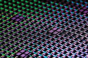
The CIRCL-AP includes multiple modules that utilize parallel data collection for fast, cost-efficient process control of advanced wafer-level packaging processes. It supports a range of packaging technologies, including wafer-level chip scale packaging, fan-out wafer-level packaging and 2.5D/3D IC integration using through silicon vias (TSVs). The industry-proven 8-Series serves as the CIRCL-AP's front side defect inspection and metrology module, which couples LED scanning technology with automated defect binning to reduce nuisance and speed detection of critical packaging defects, such as TSV cracks and redistribution layer shorts. The CV350i module, based on KLA-Tencor's VisEdge(®) technology, enables leading detection, binning and automated review of wafer edge defects and metrology for critical edge trim and bonding steps in the TSV process flow. With multiple imaging and illumination modes, the Micro300 module can produce high precision 2D and 3D metrology for bump, redistribution and TSV processes. Utilizing a flexible architecture, the CIRCL-AP can be configured with one or more modules to address the requirements of specific packaging applications, while the handler supports bonded, thinned and warped substrates.
The ICOS T830 extends the industry-leading ICOS component inspection series to address yield challenges associated with advanced packaging types, including lead frame, fan-out wafer-level, flip-chip and stacked packages. Enhanced package visual inspection capability, xPVI(TM), enables high sensitivity detection of top and bottom component surface defects, such as voids, scratches, pits, chips and exposed wires. To ensure quality standards are being met for leading-edge memory and logic packaged devices, the ICOS T830 offers high speed 3D ball, lead and capacitor metrology, package z-height measurement and component side inspection. The xCrack+ inspection station enables accurate detection of micro-crack defects--a key failure mechanism of thinner components used in mobile applications. The ICOS T830 incorporates high-throughput operation of four independent inspection stations and high-speed sorting of the inspected packaged components to achieve cost-effective component quality control.
Multiple CIRCL-AP systems in various configurations have been installed worldwide for use in development and production of TSV, fan-out wafer-level packaging and other wafer-level packaging technologies. ICOS T830 systems are in use at many worldwide IC packaging facilities, providing accurate feedback on package quality across a range of device types and sizes. To maintain the high performance and productivity demanded by semiconductor packaging providers, the CIRCL-AP and ICOS T830 systems are backed by KLA-Tencor's global, comprehensive service network. More information on the CIRCL-AP and ICOS T830 can be found on the packaging process control web page.
About KLA-Tencor:
KLA-Tencor Corporation, a leading provider of process control and yield management solutions, partners with customers around the world to develop state-of-the-art inspection and metrology technologies. These technologies serve the semiconductor, LED and other related nanoelectronics industries. With a portfolio of industry-standard products and a team of world-class engineers and scientists, the company has created superior solutions for its customers for nearly 40 years. Headquartered in Milpitas, Calif., KLA-Tencor has dedicated customer operations and service centers around the world. Additional information may be found at http://www.kla-tencor.com (KLAC-P).
CONTACT:
Investor Relations:
Ed Lockwood
Sr. Director, Investor Relations
(408) 875-9529
ed.lockwood@kla-tencor.com
Media Relations:
Meggan Powers
Sr. Director, Corporate Communications
(408) 875-8733
meggan.powers@kla-tencor.com