GaN-on-Diamond Wafer has gallium facing surface.
Share:
Press Release Summary:
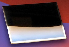
Gallium-facing GaN-on-diamond semiconductor wafer features single GaN layer atomically attached to freestanding, 25 micron thick, polycrystalline CVD diamond substrate. Nanometer proximity of chip's active region to diamond reduces heat build-up by extricating heat from core at instant of generation, permitting high temperature resilience. Measuring 10 mm², wafer has atomically smooth gallium facing surface and is shipped freestanding or optionally on disposable silicon wafer mount.
Original Press Release:
Group4 Labs' Develops Gallium Nitride-on-Diamond® Wafer with New Orientation
April 5, 2006 - Menlo Park, CA - Group4 Labs, LLC, an extreme materials developer and supplier, announces a gallium (Ga)-facing gallium nitride (GaN)-on-diamond semiconductor water. The new 10 mm² Ga-facing wafer is the third product in the Xero Wafer(TM) family and shares the same proprietary technology that permits a single GaN layer to be atomically attached to a synthetic diamond substrate. All three products exhibit unprecedented high temperature resilience for very high-power, high-frequency electronic, solid-state white lighting, military and photonics applications. Group4 Labs' semiconductor wafers are ideal for use in the conventional epitaxial growth of GaN and its aluminum and indium-based alloys.
The GaN-on-diamond, ground-breaking technology enables the GaN layer to be atomically attached to a freestanding, proprietary polycrystalline chemical-vapor-deposited (CVD) diamond substrate (25-microns thick). The new wafer's GaN exterior is an atomically smooth finish with a gallium-facing surface that is epi-ready for further epitaxial deposition. The wafer is shipped freestanding or optionally on a disposable, silicon wafer mount to allow easy handling during wafer processing.
The GaN-on-Diamond wafer addresses the classic heat problem plaguing the high power and high-speed transistor industry: excessive heat build-up inside the chip's engine that ultimately leads to device failure. The new wafer offers a unique solution by extricating heat from the chip's core almost at the instant that it is generated. This is due to the sub-nanometer proximity of the chip's active region to diamond, a nearly perfect thermal conductor. CVD diamond's thermal conductivity is about 3X to 30X more than that of conventional semiconductors. Just a 3X improvement in the thermal conductivity of a transistor array's substrate could boost the array's power-density by 10X to 100X depending on device configuration. Group4 Labs' scientists have for the first time, successfully attached a compound semiconductor such as GaN to the tough-to-handle diamond.
According to Group4 Labs' CEO, Felix Ejeckam, "This wafer features a Gallium-facing surface rather than the Nitrogen-facing surface which we introduced last month". He continues, "Unlike the optional N-facing version, this new surface resembles the conventional crystallographic structure that many of our customers are accustomed to using."
The new 10mm x 10mm GaN-on-Diamond wafers are currently sold for $550-$600 per unit (depending on quantity) through the company's online store (www.Group4Labs.com/Products).
Group4 Labs, LLC (Menlo Park, CA) is an extreme materials company founded in April 2003. The privately-held company develops and manufactures unusual semiconductor materials for a wide variety of applications in the advanced electronics and photonics industries. For more information, please visit www.Group4Labs.com.