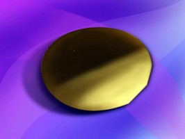
Gallium Nitride-on-Diamond® Wafer has 2 in. diameter.
Share:
Press Release Summary:

GaN-on-diamond semiconductor wafer features single GaN layer atomically attached to freestanding, 25 micron thick, polycrystalline CVD diamond substrate. Nanometer proximity of chip's active region to diamond reduces heat build-up by extricating heat from core at instant of generation, permitting high temperature resilience for high-power, high-frequency electronic, solid-state white lighting, military, and photonics applications.
Original Press Release:
Group4 Labs Extends Ground-Breaking Gallium Nitride-on-Diamond® Wafer to 2-Inches
March 31, 2006 - Menlo Park, CA - Group4 Labs, LLC, an extreme materials developer and supplier, announces the world's first 2-inch gallium nitride (GaN)-on-diamond semiconductor wafer. The new 2-inch version of the recently introduced 10 x 10 mm GaN is the second product in the company's Xero Wafer(TM) family. Sharing the same breakthrough technology, the larger GaN-on Diamond wafer also features a single GaN layer (2-inches in diameter) atomically attached to a synthetic diamond substrate (also 2-inches in diameter). This permits unprecedented high temperature resilience for very high-power, high-frequency electronic, solid-state white lighting, military and photonics applications. The two-inch wafer is ideal for use in the conventional epitaxial growth of GaN and its aluminum and indium-based alloys.
The company's innovative technology enables the GaN layer to be atomically attached to a freestanding, proprietary, polycrystalline chemical-vapor-deposited (CVD) diamond substrate (25-microns thick). The GaN exposed is an atomically-smooth surface finish that is epi-ready for further epitaxial deposition. The device is commercially available as a freestanding 2-inch wafer or optionally on a disposable, silicon substrate to permit easy handling during wafer processing.
Group4 Labs' proprietary GaN-on-Diamond technology addresses the classic heat problem plaguing the high power and high-speed transistor industry: excessive heat build-up inside the chip's engine that ultimately leads to device failure. The new material system offer a unique solution by extricating heat from the chip's core almost at the instant that it is generated. This is due to the nanometer proximity of the chip's active region to diamond, a nearly perfect thermal conductor. CVD diamond's thermal conductivity is about 3X to 30X more than that of conventional semiconductors. Just a 3X improvement in the thermal conductivity of a transistor array's substrate could boost the array's power-density by 10X to 100X depending on device configuration. Group4 Labs' scientists have, for the first time, successfully attached a 2-inch gallium nitride compound semiconductor to the tough-to-handle diamond substrate.
According to Group4 Labs' CEO, Felix Ejeckam, "This wafer is a 2-inch extension of what we introduced last month." He continues, "It's specially targeted to makers of power amplifiers (for cellular base stations), microwave and millimeter-wave circuits, UV laser diodes and ultra-bright blue/green/white LEDs who want tremendous power and thermal performance at little or no additional cost, compared to currently available semiconductor solutions."
The new GaN-on-Diamond 2-inch wafers are currently sold for $5,000 - $7,000 per unit (depending on quantity) through the company's online store at www.Group4Labs.com/Products.
Group4 Labs, LLC (Menlo Park, CA) is an extreme materials company founded in April 2003. The privately-held company develops and manufactures extreme semiconductor materials for a wide variety of applications in the advanced electronics and photonics industries. For more information, please visit www.Group4Labs.com.
GROUP4 LABS, LLC
1600 Adams Drive, Suite 112
Menlo Park, CA 94025
Phone: 1-650-688-5760 X 1
Website: www.Group4Labs.com
email: sales@Group4Labs.com, technology@Group4Labs.com


