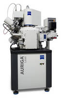
FIB/SEM, Ablation Laser accelerates sample preparation.
Press Release Summary:

Suited for examination of samples where target structure is deeply buried under material layers, AURIGA® Laser combines advantages of AURIGA® CrossBeam (FIB-SEM) workstation with capabilities of pulsed micro-focus laser. Scanning laser is nanosecond pulsed, diode-pumped, solid-state laser operating at 355 nm. Retrieving target structure is achieved automatically, and laser is equipped with CAD software controlling scanner head to realize specific ablation patterns.
Original Press Release:
Auriga® Laser: Innovative Combination of FIB/SEM Technology with Laser Ablation for Fast Sample Preparation
An innovative configuration of the proven AURIGA® CrossBeam (FIB-SEM) workstation combines a pulsed micro-focus laser for fast ablation of material with proven FIB-SEM technology. New applications and an awesome improved workflow for numerous tasks.
Today, Carl Zeiss has launched the AURIGA® Laser, a new advanced system combining the specific advantages of the AURIGA® CrossBeam (FIB-SEM) workstation with the capabilities of a pulsed micro-focus laser for fast ablation of material. AURIGA® Laser is particularly useful for the examination of samples where the target structure is deeply buried under material layers. To gain access to the target structure this material needs to be removed - a procedure which is difficult to conduct with conventional techniques. Mechanical ablation and cross-sectioning of large material volumes often cause deformations, making the sample unsuitable for further examination. In contrast, applying a focused ion beam is inefficient, because the process is much too slow.
Ablation with a pulsed micro-focus laser beam offers clear advantages: it does not damage the sample, and it enables ablation rates comparable to mechanical removal.
The scanning laser used in this unique solution is a nanosecond pulsed, diode-pumped solid-state laser operating at 355 nm provided by TRUMPF AG (Ditzingen, Germany). It was chosen from a broad range of different types of lasers to optimally meet the demands of preparing structures for SEM examination. In cooperation with Carl Zeiss, researchers from the Fraunhofer-Institute for Non-destructive Testing (IZFP - Fraunhofer-Institut für Zerstörungsfreie Prüfverfahren) in Dresden, have optimized the workflow of the innovative tool - ease of use, fast transfer procedures and fast relocation of the region of interest on the sample under examination, took center stage in the cooperation.
In order to protect the AURIGA FIB-SEM workstation and detectors from debris generated during the laser ablation process, the system is equipped with a separate chamber for laser operation. After preparing the structure of interest with the laser the sample is transferred under vacuum conditions to the main chamber for SEM examination or FIB polishing. Retrieving the target structure is achieved automatically. The transfer is carried out quickly and smoothly in a matter of seconds - resulting in a very simple and continuous workflow. To realize specific ablation patterns, the laser is equipped with CAD software controlling the scanner head. This enables the user to pre-define even highly complex patterns of the sample structure.
AURIGA® Laser is the first such instrument on the market. Dr. Martin Kienle, Director CrossBeam product line at Carl Zeiss, is convinced: "AURIGA® Laser is a milestone in simplifying the SEM examination of a vast range of innovative materials and structures, overcoming the limitations of conventional preparation methods. It enables the users to carry out new applications and to examine complex structures like next-generation nano-technology processors or flexible thin film solar cells." Future applications comprise semiconductor manufacturing, photovoltaics, polymer electronics, joining and contacting technologies, oil and gas prospection, geomechanical consulting, pharmaceuticals, life sciences and materials research in general. The system is also suitable for the preparation of microsystems that contain soft or brittle phases, such as foams, lightweight construction materials, glass fibers or ceramics, composite materials, pore filters, batteries, fuel cells or geological samples.
About Carl Zeiss
Carl Zeiss Microscopy, LLC, offers microscopy solutions and systems for research, routine, and industrial applications. In addition, Carl Zeiss Microscopy markets microscopy systems for the clinical market, as well as optical sensor systems for industrial and pharmaceutical applications. Since 1846, Carl Zeiss has remained committed to enabling science and technology to go beyond what man can see. Today, Carl Zeiss is a global leader in the optical and opto-electronic industries.
With 12,872 current employees and offices in over 30 countries, Carl Zeiss is represented in more than 100 countries with production centers in Europe, North America, Central America and Asia. For more information on the breadth of solutions offered by Carl Zeiss Microscopy, please visit http://www.zeiss.com/micro.


