Electroplating Systems handle
Press Release Summary:
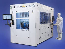
To optimize Through Silicon Via (TSV) and Through Wafer Via (TWV) processes, Solstice® electroplating systems provide plating for MEMS, sensors, RF, interposers, and other technologies for ≤200 mm wafers. Flexibly configurable solution combines chambers for critical blind via pre-wet operation with copper plating on automation frame. Solstice can routinely produce fully filled or lined vias with widths ranging from 5–250 micron having aspect ratios as high as 9:1.
Original Press Release:
ClassOne Develops New Solstice Solution for
KALISPELL, Mont. -- Semiconductor equipment manufacturer ClassOne Technology today announced a configuration for optimizing Through Silicon Via (TSV) and Through Wafer Via (TWV) processes on its affordable Solstice® electroplating systems. The Solstice family, introduced last year, is designed to provide advanced yet cost-efficient plating for MEMS, Sensors, RF, Interposers and other emerging technologies for
"In recent months customer requests for TWV, whether alone or in combination with forming redistribution layers (RDL), have skyrocketed," said Kevin Witt, ClassOne's Chief Technology Officer. "Many of our smaller-wafer customers seek the advantages of 2.5 and 3D packaging needed for their next generation products; and cost-effective TSV or TWV processing is mission critical. The new Solstice configuration addresses their needs effectively and elegantly with a plating tool that is affordably priced for 200mm and smaller substrates."
Witt explained that the new Solstice TSV configuration, which has already been sold to customers, employs a unique, high-efficiency but simple vacuum pre-wet chamber followed by copper via electroplating. This combination of capabilities enables the ClassOne tool to routinely produce fully-filled or lined vias with widths ranging from 5 to 250 micron having aspect ratios as high as 9:1. Traditionally, this level of performance has been challenging even for plating systems costing twice as much as Solstice. The Solstice can also be configured to perform additional downstream processing such as resist strip and seed layer etch making it a cluster tool that delivers a suite of critical processes, reducing cycle time and saving money. This technology makes it possible to process TSV alone or TSV and redistribution layers simultaneously to provide a complete solution on a single tool.
"New customers always have the same reaction when they first see our Solstice platers in action," said Byron Exarcos, President of ClassOne. "They're always amazed that tools this affordable deliver such advanced processing. The new Solstice TSV configuration is one more example of what is making Solstice the preferred solution for electroplating on smaller wafers!"
Designed for high-performance, cost-efficient
For additional information about the Solstice electroplating product line, TSV plating or ClassOne Technology, visit www.classone.com.
About ClassOne Technology
ClassOne Technology (www.classone.com/) develops and delivers innovative new wet-chemical equipment solutions especially for the cost-conscious users of smaller substrates, who traditionally have been underserved by the larger equipment manufacturers. Based in Kalispell, Montana, ClassOne Technology is built upon many decades of experience from industry veterans who continue the ClassOne tradition of delivering quality and performance at an affordable price. ClassOne Technology is a sister company to ClassOne Equipment (ClassOneEquipment.com), long respected as the industry's premier provider of refurbished processing tools, with over 2,500 systems installed worldwide.
For more information, contact:
Byron Exarcos
ClassOne Technology
109 Cooperative Way, #101
Kalispell, MT 59901
tel: +1 (678) 772-9086
Solstice® is a registered trademark of ClassOne Technology.